Method and system for optimizing chip area and power consumption

A chip area and optimization method technology, applied in the direction of instruments, input/output to record carrier, calculation, etc., can solve the problems of register waste, chip area resource waste, execution unit limitation, etc., to improve performance and power consumption ratio, ensure Effects of functional correctness, area and power reduction

Active Publication Date: 2021-03-05
上海睿伍科技有限公司
View PDF6 Cites 0 Cited by
  • Summary
  • Abstract
  • Description
  • Claims
  • Application Information

AI Technical Summary

Problems solved by technology

[0005] However, in the current data flow structure processor and some heterogeneous computing acceleration processors, some storage adopts the register structure, such as the instruction storage module, but due to the limitation of the execution unit in these processors, it is impossible to execute a large number of instructions in one clock cycle. Instead, it can only execute a few instructions, and the instruction storage module stores hundreds of instructions, so it does not make full use of the characteristics of register independent reading, which is a waste of using registers and a waste of precious area resources of the chip. , since the area is proportional to the power consumption, it also causes waste of power consumption

Method used


Image

  • Method and system for optimizing chip area and power consumption
  • Method and system for optimizing chip area and power consumption
  • Method and system for optimizing chip area and power consumption

Examples


Embodiment Construction

[0037] The present invention will be described in detail below with reference to the accompanying drawings and examples. It should be noted that, in the case of no conflict, the embodiments in the present application and the features in the embodiments can be combined with each other.

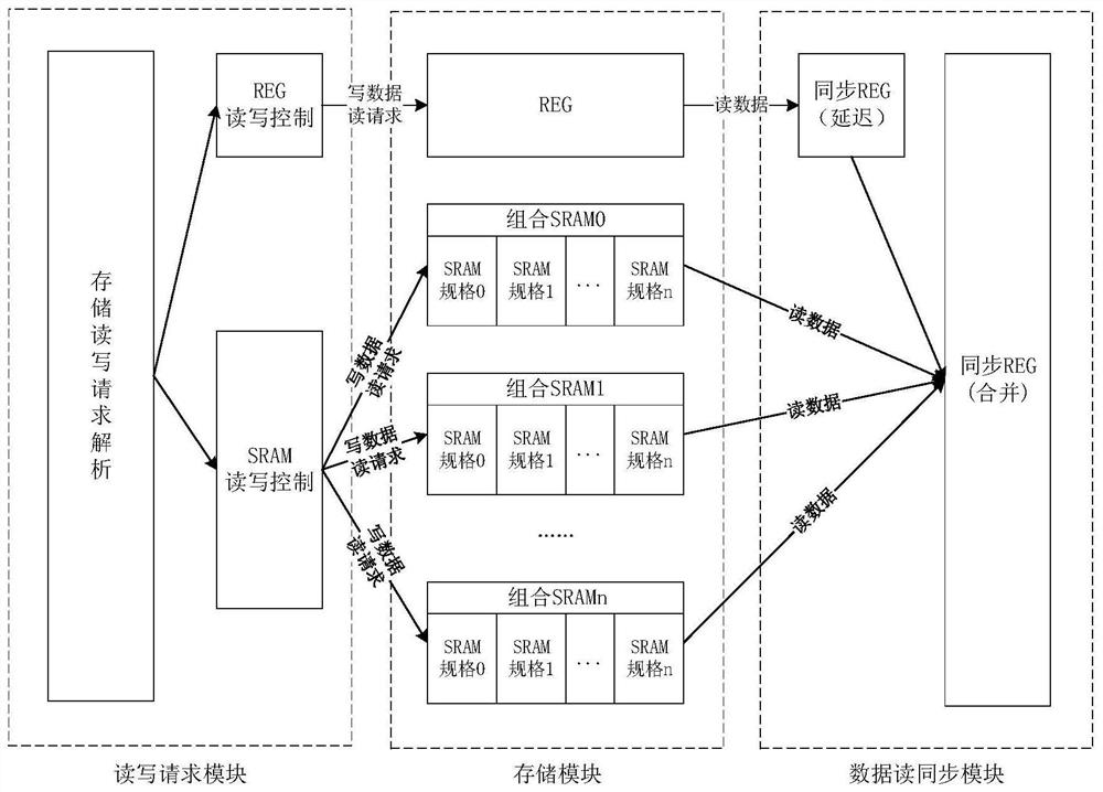
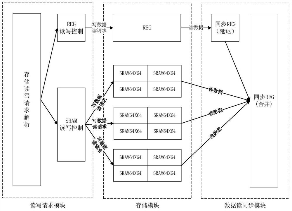
[0038] Such as figure 1 As shown, it is a schematic diagram of an example result of a chip area and power consumption optimization system of the present invention. A chip area and power consumption optimization system of the present invention includes: a read-write request module, a storage module and a data synchronization module. The main function of the read and write request module is to analyze the read and write requests, send the requests to the register and the SRAM read and write control module, and analyze the number of reads and writes in a single clock cycle of the register. The write data to the combined SRAM0-n is consistent, While read requests are independent. The main functio...


PUM


Abstract

The invention provides a chip area and power consumption optimization method and system. The chip area and power consumption optimization method includes the following steps of analyzing the read-write frequency within a single clock cycle of a register; if the read-write frequency within the single clock cycle of the register is low, carrying out SRAM specification selection; substituting the register with an SRAM; carrying out data reading synchronization. The chip area and power consumption optimization method and system can effectively reduce the area and power consumption of a processor and meanwhile generate less influences on the performance, and therefore the overall performance power consumption ratio of the processor is improved.

Description

technical field [0001] The invention relates to the field of chip design and structure optimization, in particular to a chip area and power consumption optimization method and system. Background technique [0002] With the development of computer architecture, the domain-specific computer architecture has become the main development trend. When facing specific applications, the special-purpose structure uses the application characteristics to optimize the structure accordingly, so as to better exert the computing performance of the hardware. In the field of high-performance computing, data flow computing is an important branch of domain-specific computing structures, and data flow computing has shown good performance and applicability. [0003] At present, the data flow structure processor chip integrates a large number of storage units. These storage units store the instructions, data and control information that need to be executed in advance, which can avoid frequent memo...

Claims


Application Information

Patent Timeline
Patent Type & Authority Patents(China)
IPC IPC(8): G06F3/06G06F1/3234
CPCG06F1/3275G06F3/061G06F3/064
Inventor 李易李涵张浩吴冬冬范东睿
Owner 上海睿伍科技有限公司
Why Eureka
Try Eureka