Gas injector device used for semiconductor equipment
A gas injection and semiconductor technology, applied in the direction of injection devices, injection devices, electrical components, etc., can solve the problem that the output gas flow rate is difficult to adjust and control in real time
- Summary
- Abstract
- Description
- Claims
- Application Information
AI Technical Summary
Problems solved by technology
Method used
Image
Examples
Embodiment Construction
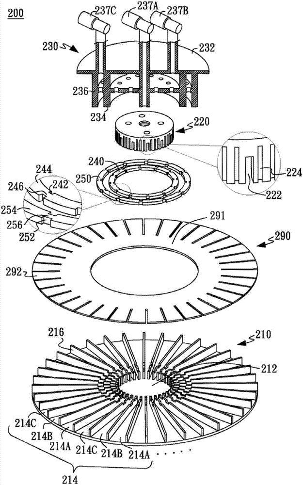
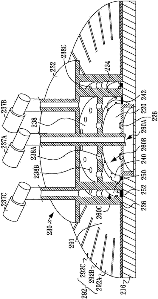
[0061] Please refer to Figure 2A and Figure 2B , Which respectively show a component exploded view and a partial cross-sectional view of a combined structure of a gas injection device applied to semiconductor equipment according to an embodiment of the present invention. As shown in the figure, a gas injection device 200 applied to semiconductor equipment includes a bottom plate 210, a center cover 220, an intake body 230, an inner ring cover 240, and an outer ring cover 250. The bottom plate 210 includes a central area 212 and a plurality of passages 214. The passages 214 are arranged adjacent to the bottom plate 210 with the central area 212 as the center. The passage 214 also includes a plurality of first passages 214A and a plurality of second passages. 214B and a plurality of third channels 214C.
[0062] The central cover 220 is disposed on the central area 212 and forms a first air inlet cavity 260A with the bottom plate 210. The ring wall of the central cover 220 is con...
PUM
| Property | Measurement | Unit |
|---|---|---|
| thickness | aaaaa | aaaaa |
Abstract
Description
Claims
Application Information


