Display device and electronic equipment

A display device and display panel technology, applied in the fields of electronic equipment and display devices, can solve the problems of complex manufacturing process, and achieve the effects of ensuring accuracy, improving stability and integration, and avoiding influence

Active Publication Date: 2018-04-06
BEIJING XIAOMI MOBILE SOFTWARE CO LTD
View PDF1 Cites 17 Cited by
  • Summary
  • Abstract
  • Description
  • Claims
  • Application Information

AI Technical Summary

Problems solved by technology

[0004] However, no matter which method is mentioned above, the fingerprint identification module needs to be manufactured separately, and then installed in the smart terminal, and the manufacturing process is relatively complicated.

Method used


Image

  • Display device and electronic equipment
  • Display device and electronic equipment
  • Display device and electronic equipment

Examples


Embodiment Construction

[0058] Reference will now be made in detail to the exemplary embodiments, examples of which are illustrated in the accompanying drawings. When the following description refers to the accompanying drawings, the same numerals in different drawings refer to the same or similar elements unless otherwise indicated. The implementations described in the following exemplary examples do not represent all implementations consistent with the present disclosure. Rather, they are merely examples of apparatuses and methods consistent with aspects of the present disclosure as recited in the appended claims.

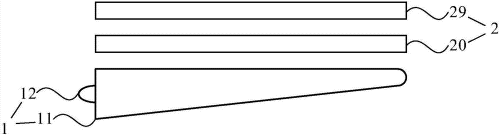
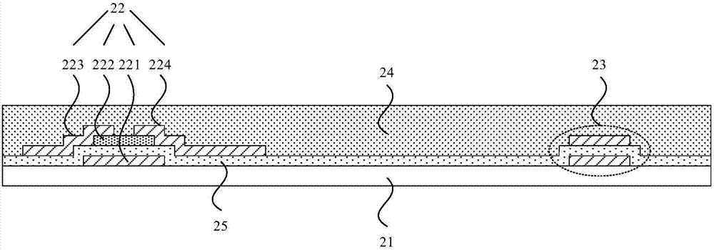
[0059] figure 1 It is a schematic structural diagram of a display device according to an exemplary embodiment. figure 2 is a schematic structural diagram of an array substrate according to an exemplary embodiment. Such as figure 1 As shown, the display device includes:

[0060] Backlight module 1, display panel 2 and control chip (not shown in the figure, can be electrically conne...


PUM


Abstract

The invention relates to a display device. The display device comprises a backlight module and an array substrate, wherein the array substrate comprises a base, thin-film transistors which are arranged in a first area at one side of the base and a photoelectric sensor which is arranged in a second area at one side of the base and is used for recognizing fingerprints according to received invisiblelight; the backlight module comprises a plurality of first light sources and at least one second light source corresponding to the second area; the second light source is used for emitting invisiblelight; when the photoelectric sensor is located a state of being about to recognize fingerprints, a control chip controls the thin-film transistor, corresponding to the second area, in the thin-film transistors and the second light source to be opened. According to the display device, the second light source corresponding to the second area is additionally arranged in the backlight module, so thatinvisible light can be emitted to be recognized by the photoelectric sensors, thereby avoiding the influences, on fingerprint recognition, of visible light in external environment and ensuring the correctness of recognition results.

Description

technical field [0001] The present disclosure relates to the field of display technology, and in particular, to a display device and an electronic device. Background technique [0002] With the diversification of encryption / decryption operations of smart terminals, fingerprints, an attribute that everyone has but varies from person to person, are getting more and more attention. Therefore, fingerprint identification modules are more and more commonly integrated in smart terminals. [0003] At present, the fingerprint identification module in the smart terminal (such as a mobile phone) mainly includes two types: the back and the front of the smart terminal. integrated together. [0004] However, no matter which method is mentioned above, the fingerprint recognition module needs to be manufactured separately, and then installed in the smart terminal, and the manufacturing process is relatively complicated. Contents of the invention [0005] The present disclosure provides ...

Claims


Application Information

Patent Timeline
Patent Type & Authority Applications(China)
IPC IPC(8): G06F3/041
CPCG06F3/0412
Inventor 江忠胜刘安昱于磊
Owner BEIJING XIAOMI MOBILE SOFTWARE CO LTD
Why Eureka
Try Eureka