Method for evaporating gold on front surface of wafer

A wafer and gold vaporization technology, which is applied in the fields of electrical components, semiconductor/solid-state device manufacturing, circuits, etc., can solve the problems of lower device yield and reliability

Inactive Publication Date: 2018-04-06
SHANGHAI HUAHONG GRACE SEMICON MFG CORP
View PDF5 Cites 2 Cited by
  • Summary
  • Abstract
  • Description
  • Claims
  • Application Information

AI Technical Summary

Problems solved by technology

[0004] The purpose of the present invention is to provide a method for vaporizing gold on the front of the wafer to solve the

Method used


Image

  • Method for evaporating gold on front surface of wafer
  • Method for evaporating gold on front surface of wafer
  • Method for evaporating gold on front surface of wafer

Examples


Embodiment Construction

[0031] The specific implementation manner of the present invention will be described in more detail below with reference to schematic diagrams. Advantages and features of the present invention will be apparent from the following description and claims. It should be noted that all the drawings are in a very simplified form and use imprecise scales, and are only used to facilitate and clearly assist the purpose of illustrating the embodiments of the present invention.

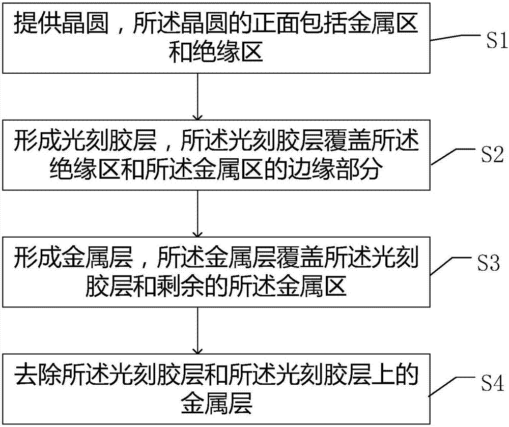
[0032] refer to figure 1 , which is a flow chart of the method for wafer front evaporation gold provided by the embodiment, such as figure 1 Shown, the method for vaporizing gold on the front side of the wafer comprises:

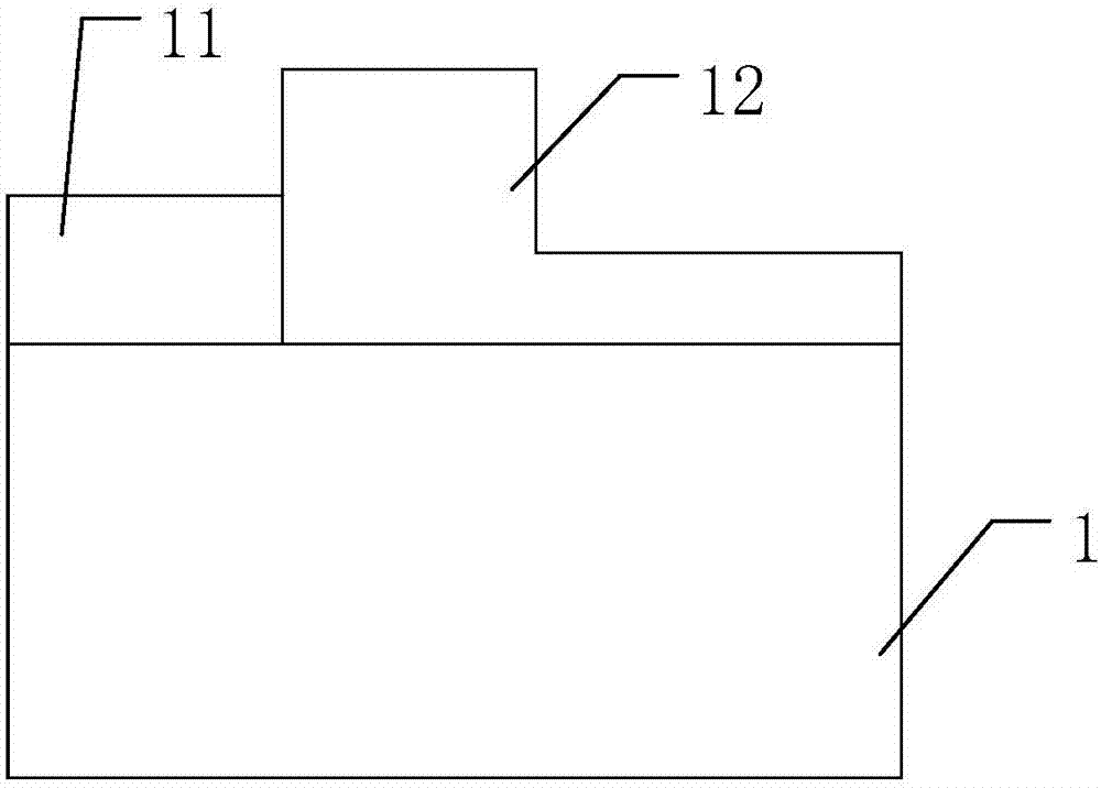
[0033] S1: providing a wafer, the front side of the wafer includes a metal region and an insulating region;

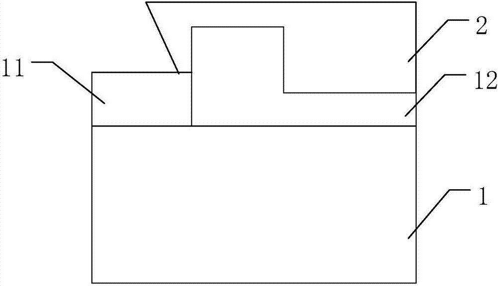
[0034] S2: forming a photoresist layer, the photoresist layer covering the edge portions of the insulating region and the metal region;

[0035] S3: forming a metal layer, the metal...


PUM


Abstract

The invention provides a method for evaporating gold on a front surface of a wafer. The method comprises the steps of forming a metal region and an insulation region on the front surface of the wafer,covering an edge part of the insulation region and the metal region with a photoresist layer, forming a metal layer on the photoresist layer and the remaining metal region, and removing the photoresist layer and the metal layer on the photoresist layer. According to the method for evaporating gold on the front surface of the wafer, the photoresist layer covers the edge part of the metal region, the metal layer is covered on the remaining metal region and the photoresist layer, the adhesive force between a metal material of front-surface metal and a metal region is larger than the adhesive force between the front-surface metal and the photoresist layer, the photoresist layer and the metal layer on the photoresist layer can be subsequently and easily removed according to the difference between the adhesive forces of the metal material on the photoresist layer and the metal, and the front-surface metal cannot be stripped or upwarped.

Description

technical field [0001] The invention relates to the field of semiconductor manufacturing, in particular to a method for vaporizing gold on the front side of a wafer. Background technique [0002] In wafer processing engineering, when manufacturing certain semiconductor devices or when manufacturing certain types of integrated circuits, it is necessary to deposit front metal on the wafer (that is, the evaporation gold process on the front of the wafer). Condition. Especially in the packaging process of power devices, a large internal thermal resistance will be introduced when the upper and lower electrodes are soldered to the chip. The front-side steam gold process can fundamentally solve this problem, reduce the forward voltage drop VF of the device, and increase the shear stress of the chip. , thereby improving the inherent reliability and thermal fatigue resistance of the chip. [0003] However, in the actual production process, the metal layer formed on the surface of t...

Claims


Application Information

Patent Timeline
IPC IPC(8): H01L21/02H01L21/027
CPCH01L21/02697H01L21/0272
Inventor 王鹏刘宇李秀莹
Owner SHANGHAI HUAHONG GRACE SEMICON MFG CORP
Why Eureka
Try Eureka