Preparation method of PCB semi-hole slices

A production method and slicing technology, which is applied in the direction of measuring devices, instruments, scientific instruments, etc., can solve the problem of inferring the drilling conditions of glass fiber cloth and resin on the hole wall, inability to fully reflect the quality information of the hole wall, and affecting the slicing hole problems such as the degree of reduction of the wall, to achieve the effect of tight combination, elimination of protective insulation layer, and high degree of reduction

Active Publication Date: 2018-04-10
GUANGDONG UNIV OF TECH
View PDF8 Cites 2 Cited by
  • Summary
  • Abstract
  • Description
  • Claims
  • Application Information

AI Technical Summary

Problems solved by technology

The sample taken is basically plated with copper on the hole wall. This method can only observe the morphology of the glass fiber cloth and resin on the grinding surface after drilling (that is, when the half hole is ground, only the half hole groove can be observed. two sides), it is difficult to speculate on the glass fiber cloth and resin drilling of the entire hole wall, and it is impossible to fully reflect the quality information of the hole wall
Of course, at present, there are also half-hole slices that have not undergone the copper-immersion copper plating process, but this method does not protect or isolate the hole wall, and it is easy to cause abrasive debris to adhere to the hole wall or even damage the shape of the hole wall during the grinding process. Affects the reduction degree of the slice hole wall

Method used


Image

  • Preparation method of PCB semi-hole slices
  • Preparation method of PCB semi-hole slices
  • Preparation method of PCB semi-hole slices

Examples


Embodiment 1

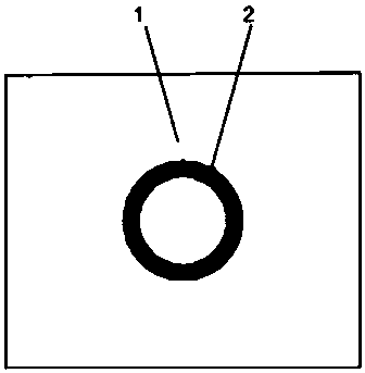
[0038] Such as Figure 1-3 As shown, the present embodiment provides a method for making a PCB half-hole slice, comprising the following steps:

[0039] S1: Add a layer of protective insulation layer 2 on the wall of hole 1 of the PCB template;

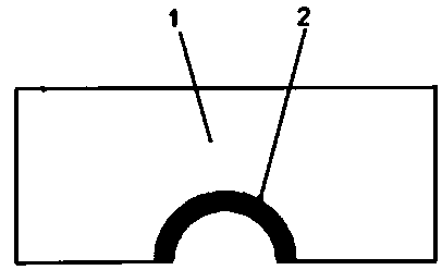
[0040] S2: Sampling the target hole with the added protective insulating layer 2, grinding until half of the hole is left, and then polishing;

[0041] S3: removing the protective insulation layer 2 on the wall of the polished half-hole section;

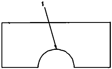
[0042] S4: Place the half-hole section after removing the protective insulating layer 2 under a scanning electron microscope and other detection equipment for observation and detection. The results are as follows: Figure 4 shown.

[0043] Adding a layer of protective insulation layer 2 on the hole wall is used to prevent the hole wall from being damaged or adhered to grinding debris during the grinding process of the half-hole slice. After completion, it can be removed under the conditi...

Embodiment 2

[0053] This embodiment provides a method for making a PCB half-hole slice, comprising the following steps:

[0054] S1: Add a layer of protective insulation layer 2 on the wall of hole 1 of the PCB template;

[0055] S2: Sampling the target hole with the added protective insulating layer 2, grinding until half of the hole is left, and then polishing;

[0056] S3: removing the protective insulation layer 2 on the wall of the polished half-hole section;

[0057] S4: Place the half-hole section after removing the protective insulating layer 2 under a scanning electron microscope and other testing equipment for observation and detection to obtain the characteristics or composition information of the half-hole wall, and then infer the entire hole wall condition.

[0058] The protective insulating layer 2 is thermoplastic resin, and the thickness of the protective insulating layer 2 is 2 μm.

[0059] The protective insulation layer 2 in step S3 is softened and eliminated by baking t...


PUM

PropertyMeasurementUnit
thicknessaaaaaaaaaa
thicknessaaaaaaaaaa

Abstract

The invention provides a preparation method of PCB semi-hole slices. The preparation method comprises following steps: S1, firstly, the hole wall of a PCB template is provided with a protective insulating layer; S2, a target hole provided with the protective insulating layer is subjected to sampling, grinding is carried out to close to semi-hole, and then polishing is carried out; S3, after polishing, the protective insulating layer of an obtained semi-hole slice hole wall is removed; S4, after removing of the protective insulating layer, the obtained semi-hole slice is subjected to observation detection using equipment such as a scanning electron microscope so as to obtain semi-hole wall characteristics or ingredient information, and then speculation of the formation situations of the whole hole wall is realized. According to the preparation method, the recovery degree of the obtained semi-hole wall is high, and speculation of whole hole wall formation situations can be realized accurately.

Description

technical field [0001] The invention relates to the field of printed circuit boards (PCBs), in particular to a method for manufacturing PCB half-hole slices. Background technique [0002] In the production process of printed circuit boards, the occurrence and solution of product quality problems and the improvement of the process need to be studied and judged by observing hole slices (PCB half-hole slices), and whether the hole slices are good or bad depends on the How high the degree of restoration of the actual hole wall is is the key factor for judging and studying the quality and process of PCB. Especially for PCB drilling with warp and weft interwoven glass fiber cloth, whether the observed hole wall information is complete and true is the key to in-depth research. [0003] At present, the production of PCB half-hole slices includes the following five steps: sampling, sealing, grinding, polishing and micro-etching. The sample taken is basically plated with copper on t...

Claims


Application Information

Patent Timeline
Patent Type & Authority Applications(China)
IPC IPC(8): G01N23/2251G01N23/2202
CPCG01N23/2202G01N23/2251
Inventor 郑李娟林淡填王成勇黄欣李之源何醒荣李浩
Owner GUANGDONG UNIV OF TECH
Why Eureka
Try Eureka