High-performance output driving circuit

An output drive circuit, output drive technology, applied in the direction of logic circuit, logic circuit connection/interface layout, logic circuit coupling/interface using field effect transistors, etc., can solve the problems of failure to restore normal value, abnormal output signal, and level conversion Circuits and buffer circuits can not work properly, to reduce sensitivity, improve reliability, and improve performance

Active Publication Date: 2018-04-20
SHANGHAI HUALI MICROELECTRONICS CORP
View PDF8 Cites 23 Cited by
  • Summary
  • Abstract
  • Description
  • Claims
  • Application Information

AI Technical Summary

Problems solved by technology

The greater the parasitic resistance, the higher the power supply voltage, and the greater the voltage change caused by the parasitic resistance. In severe cases, even the level shifting circuit and buffer circuit of the previous stage cannot work normally, causing the output control signals PS and NS to be embedded. At an interm

Method used


Image

  • High-performance output driving circuit
  • High-performance output driving circuit
  • High-performance output driving circuit

Examples


Embodiment Construction

[0028] The embodiments of the present invention will be described below through specific examples and in conjunction with the accompanying drawings, and those skilled in the art can easily understand other advantages and effects of the present invention from the contents disclosed in this specification. The present invention can also be implemented or applied through other different specific examples, and various details in this specification can also be modified and changed based on different viewpoints and applications without departing from the spirit of the present invention.

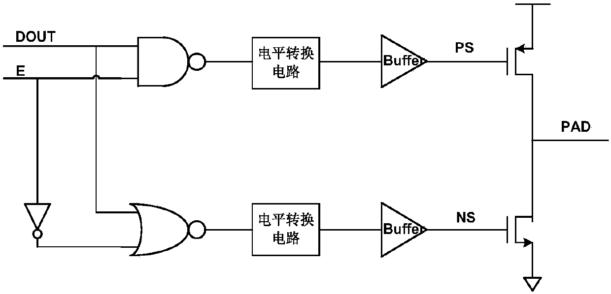
[0029] image 3 It is a circuit structure diagram of a high-performance output driving circuit of the present invention. like image 3 As shown, a high-performance output drive circuit of the present invention includes: an output logic unit 10, a level conversion unit 11, a buffer unit 12, and an output drive tube 13.

[0030]Among them, the output logic unit 10 is composed of a NOT gate NOT1, a N...


PUM


Abstract

The invention discloses a high-performance output driving circuit, which comprises an output logic unit, a level conversion unit, a buffer unit and an output stage, wherein the output logic unit is used for converting DOUT output by a chip core into two paths of controlled output signals under the control of an enable signal E; THE level conversion unit is used for converting the two paths of controlled output signals with low power supply voltage level of the chip core into two paths of controlled high-voltage output signals with high power supply voltage level of an IO interface circuit, andoutputting the two paths of controlled high-voltage output signals to the buffer unit; the buffer unit is used for increasing driving capacity stage by stage, so as to drive a large-size MOS transistor of the output state; and the output stage is used for transmitting an output signal OUT to a welding pad so as to provide a driving current required for driving a peripheral circuit, and driving anoutput load. By adopting the high-performance output driving circuit, the influence of voltage variations of a parasitic resistor on the operation of an entire output circuit can be effectively reduced when a parasitic capacitor is being charged and discharged by means of a high power supply voltage VCCIO and ground VSSIO of the IO interface circuit, and the reliability of operation of the outputcircuit can be improved.

Description

technical field [0001] The invention relates to an output driving circuit, in particular to a high-performance output driving circuit. Background technique [0002] The IO interface circuit (input and output interface circuit) is widely used in various types of IP circuits, and the normal operation of the IO circuit directly determines the availability of the entire IP circuit. [0003] figure 1 A commonly used prior art output driver circuit is shown, the circuit includes an output logic part, a level conversion part, a buffer part and an output driver tube, wherein the buffer part is only composed of an even number of inverters. The current large-scale integrated circuit signals are becoming more and more complex, and the required PIN pins are increasing. For example, chips such as SRAM only have dozens of input and output PINs, while the overall number of IOs on the chip is limited, and some output PINs are far away from VCCIO and VSSIO PINs. Metal traces are long and i...

Claims


Application Information

Patent Timeline
IPC IPC(8): H03K19/0185H03K19/003
CPCH03K19/00315H03K19/018507
Inventor 刘雯胡晓明浦珺慧
Owner SHANGHAI HUALI MICROELECTRONICS CORP
Why Eureka
Try Eureka