A silicon carbide linear temperature sensor, temperature measurement method and manufacturing method thereof

A technology of temperature sensor and silicon carbide, which is applied in thermometers, thermometers with directly heat-sensitive electric/magnetic elements, instruments, etc., can solve the problems of integrated crosstalk and low sensitivity of main devices, and achieve the goal of reducing crosstalk, improving sensitivity, The effect of a large temperature range

Active Publication Date: 2019-12-27
UNIV OF ELECTRONICS SCI & TECH OF CHINA
View PDF11 Cites 0 Cited by
  • Summary
  • Abstract
  • Description
  • Claims
  • Application Information

AI Technical Summary

Problems solved by technology

[0015] The technical problem to be solved by the present invention is to provide a silicon carbide temperature sensor with a dual Schottky diode structure for the low sensitivity of the silicon carbide temperature sensor for temperature monitoring and serious crosstalk with the main device. Introducing the diffusion resistance R s The linear dependence with temperature improves the sensitivity of the device; at the same time, the device structure proposed by the present invention is a horizontal structure, which is easier to integrate than the existing vertical structure

Method used


Image

  • A silicon carbide linear temperature sensor, temperature measurement method and manufacturing method thereof
  • A silicon carbide linear temperature sensor, temperature measurement method and manufacturing method thereof
  • A silicon carbide linear temperature sensor, temperature measurement method and manufacturing method thereof

Examples


Embodiment 1

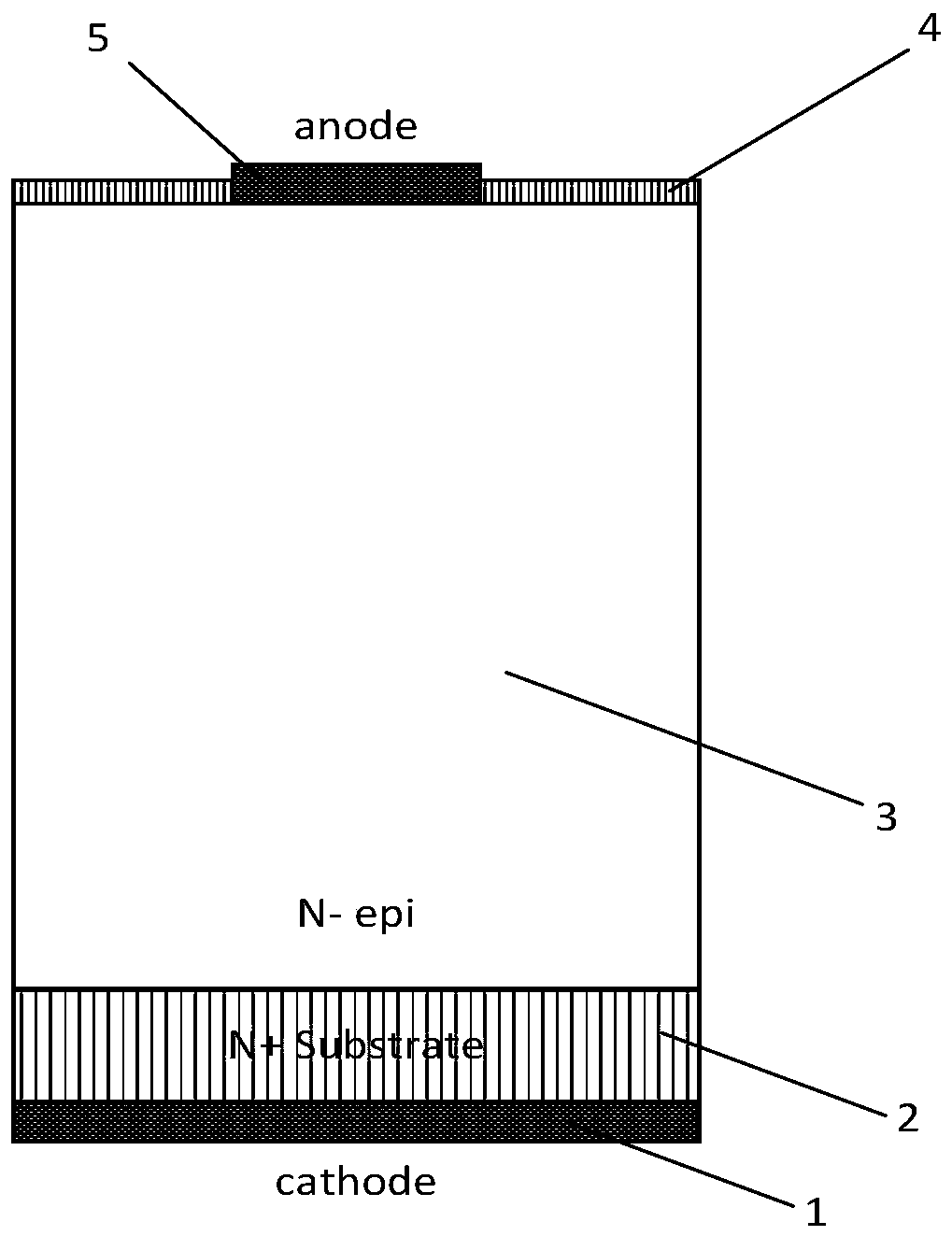
[0061] Such as figure 1 Shown is a SiC SBD temperature sensor with a traditional vertical structure. In order to compare its performance with the temperature sensor of the present invention, this embodiment adopts the same doping level to make a vertical SiC SBD temperature sensor, as follows: silicon carbide N- epitaxial layer The doping concentration of 2 is 2E17cm -3 Yes, the thickness of the silicon carbide N- epitaxial layer 2 is 10 microns, the metal Ti / Al alloy is used as the Schottky contact electrode 8, and the metal Ni is used as the ohmic contact electrode 7.

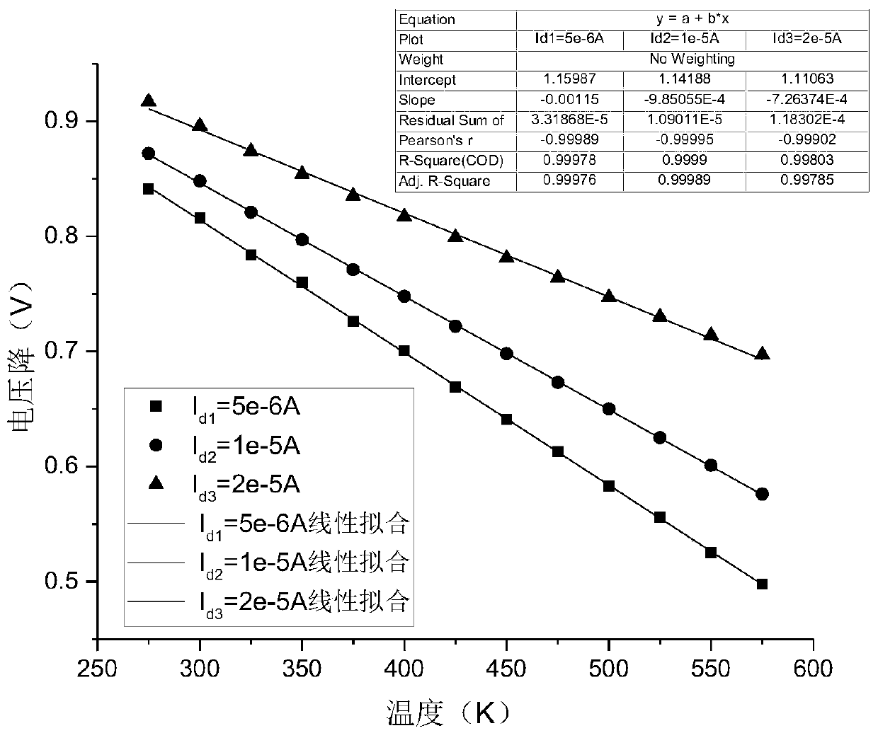
[0062] This embodiment adopts TCAD software Silvaco to build such as figure 1 device structure, in order to obtain its V-T characteristic curve, its Schottky contact electrode 8 is respectively biased with a constant current of 5E-6A, 1E-5A and 2E-5A, when the current through the SBD is constant, its Xiao The forward voltage drop on the TG barrier will change linearly with the temperature. Using this princi...

Embodiment 2

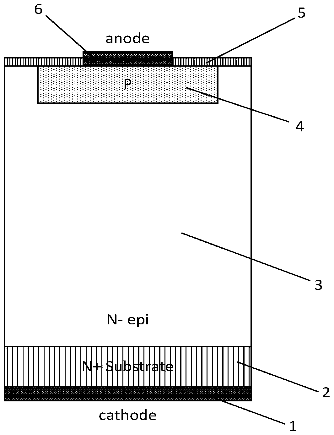
[0064] Such as image 3 Shown is a SiC PN junction temperature sensor with a traditional vertical structure. In order to compare its performance with the temperature sensor of the present invention, this embodiment adopts the same doping level to make a vertical SiC PN temperature sensor, as follows: silicon carbide N-epitaxy The doping concentration of layer 2 is 2E17cm -3 The thickness of the silicon carbide N-epitaxial layer 2 is 10 microns, the metal Al is used as the Schottky contact electrode 8, the metal Ni is used as the ohmic contact electrode 7, and the doping concentration of the P well region 3 is 2E17cm -3 , the thickness of the P well region 3 is 2 microns.

[0065] This embodiment adopts TCAD software Silvaco to build such as image 3 In order to obtain its V-T characteristic curve, its ohmic contact electrode 7 is respectively biased with a constant current of 5E-5A, 1E-4A and 2E-4A. When the current passing through the PN junction is constant, its PN junctio...

Embodiment 3

[0067] Such as Figure 5 Shown is a specific embodiment of the SiC temperature sensor with a lateral double SBD structure provided by the present invention, which is characterized in that it includes a silicon carbide N+ substrate 1, and a silicon carbide N+ substrate 1 is provided above the silicon carbide N+ substrate 1. - epitaxial layer 2, the SiC N - The center of the top layer of the epitaxial layer 2 has a P well region 3, the center of the top layer of the P well region 3 has an N well region 4, and the middle position of the top layer of the N well region 4 has an N-type silicon carbide ohmic contact region 5, and the N-type silicon carbide ohmic contact region An ohmic contact electrode 7 connected to it is arranged on the top of the region 5, and two Schottky contact electrodes 8 connected thereto and arranged symmetrically above the two ends of the top layer of the N well region 4, the two Schottky contact electrodes 8 and The ohmic contact electrodes 7 are indepe...


PUM

PropertyMeasurementUnit
depthaaaaaaaaaa
depthaaaaaaaaaa
thicknessaaaaaaaaaa

Abstract

A silicon carbide linear temperature sensor, a temperature measuring method and a manufacturing method thereof belong to the technical field of semiconductor devices. The present invention includes silicon carbide N ‑ The P well on the top layer of the epitaxial layer, the N well with a shallower junction depth in the center of the top layer of the P well, the N-type silicon carbide ohmic contact area in the center of the N well, the ohmic contact electrode located on the upper surface of the N-type silicon carbide ohmic contact area, and the N well N-type Schottky contact electrodes at both ends and a passivation layer on the surface of the device. The present invention adopts a horizontal design to obtain a silicon carbide temperature sensor based on a double Schottky diode structure. On the one hand, it can eliminate the influence of the reverse saturation current on the linearity of the sensor and improve its linearity. On the other hand, it introduces a diffusion resistance R s The linear dependence with temperature improves the sensitivity of the device; at the same time, the device structure proposed by the present invention is a horizontal structure, which is easier to integrate than the existing vertical structure, and the crosstalk between the main sensor devices can be reduced by the isolation of the P well , increasing the feasibility of its integration with N-type epitaxial power devices.

Description

technical field [0001] The invention belongs to the technical field of semiconductor devices, in particular to a silicon carbide linear temperature sensor, a temperature measuring method and a manufacturing method thereof. Background technique [0002] Wide bandgap semiconductor material—silicon carbide (SiC) is an ideal material for preparing high-voltage power electronic devices. Compared with Si materials, SiC materials have a higher breakdown electric field strength (4×10 6 V / cm), high carrier saturation drift velocity (2×10 7 cm / s), high thermal conductivity, and good thermal stability, so it is especially suitable for high-power, high-pressure, high-temperature and radiation-resistant electronic devices. [0003] SiC VDMOS devices are more commonly used in SiC power devices. Compared with bipolar devices, SiC VDMOS devices have better frequency characteristics and lower switching losses because they have no charge storage effect. At the same time, the wide bandgap of...

Claims


Application Information

Patent Timeline
Patent Type & Authority Patents(China)
IPC IPC(8): G01K7/01H01L29/47H01L29/872
CPCG01K7/015H01L29/47H01L29/872
Inventor 张有润顾航陈航路统霄胡刚毅李俊焘张波
Owner UNIV OF ELECTRONICS SCI & TECH OF CHINA
Why Eureka
Try Eureka