PCI pin digital microfluidic chip based on double-layer pcb and its method

A technology of digital microfluidics and PCB boards, which is applied in fluid controllers, chemical instruments and methods, and laboratory containers. It can solve problems such as poor electrical connections, difficult chip fixing, and normal use of equipment, and achieve reliable mechanical Fixation, increase density, reduce crowding effect

Active Publication Date: 2020-12-29
DALIAN INST OF CHEM PHYSICS CHINESE ACAD OF SCI
View PDF8 Cites 0 Cited by
  • Summary
  • Abstract
  • Description
  • Claims
  • Application Information

AI Technical Summary

Problems solved by technology

Usually, the fixing and electrical connection of the chip are realized by the chip fixture and the chip test clip respectively, but in actual operation, it is easy to have problems such as the position of the chip is not easy to fix, and the electrical connection is poor, which affects the normal use of the equipment

Method used


Image

  • PCI pin digital microfluidic chip based on double-layer pcb and its method
  • PCI pin digital microfluidic chip based on double-layer pcb and its method
  • PCI pin digital microfluidic chip based on double-layer pcb and its method

Examples


Embodiment Construction

[0030] The present invention will be further described in detail below in conjunction with the accompanying drawings and embodiments.

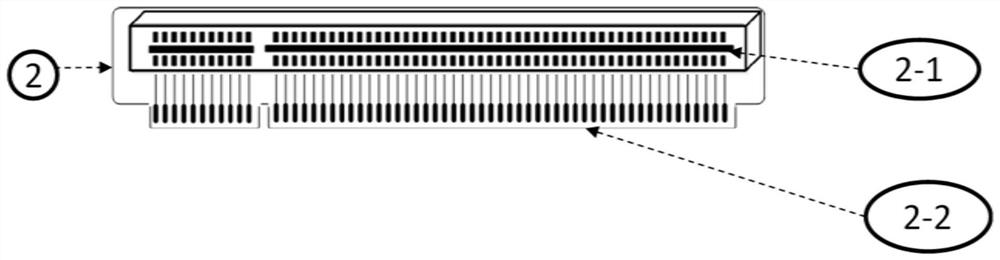
[0031] PCI is a standard parallel communication bus used in computer hardware. By setting a PCI connector on the computer motherboard, peripheral hardware, such as memory sticks, display cards, etc., can be connected. The main feature of the PCI connector is that the connector has 2 slots, of which the short slot and the long slot provide 22 reeds and 50 reeds that are electrically independent of each other, so it can provide many parallel interfaces. High interface density and fast data transmission. For example, a conventional PCI connector based on a double-layer PCB structure has a golden finger interface pitch of 1.27mm and can provide up to 144 parallel input or output channels at a width of 85mm.

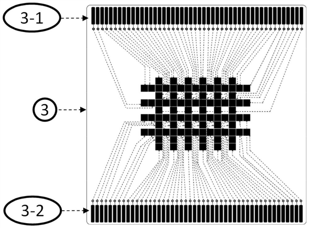
[0032] The present invention provides a digital microfluidic chip design based on a double-layer PCB, and the planar structure schematic d...


PUM


Abstract

The invention relates to a PCI (peripheral component interconnect) pin digital microfluidic chip based on double PCB layers. The PCI pin digital microfluidic chip based on the double PCB layers is characterized by comprising an upper electrode plate, a lower electrode plate and a PCI slot, wherein both the upper electrode plate and the lower electrode plate are PCBs; and gold finger pins are arranged at edges of the upper electrode plate and the lower electrode plate and inserted into the PCI slot. The method comprises the following steps: liquid drops are added dropwise to electrodes on the lower electrode plate, and a liquid column is formed between the upper electrode plate and the lower electrode plate; a control system applies liquid drop driving voltage to electric pins connected with adjacent electrodes of the liquid drops through the PCI slot, and the liquid drops are driven to move to the adjacent electrodes. With adoption of the double-PCB structure, leads are arranged on theback side of the chip, so that interference of electrified leads in movement of the liquid drops is avoided, and occupation of limit front space of the chip by the leads is reduced to the greatest extent, so that density of working electrodes of the digital microfluidic chip is increased greatly.

Description

technical field [0001] The invention relates to electrical engineering and microfluidic chip technology, and in particular provides a PCI pin digital microfluidic chip based on a double-layer PCB and a working method thereof. Background technique [0002] The droplet microfluidic chip is an important branch of the field of microfluidic chips. Two immiscible liquids, one of which is used as the continuous phase, and the other is used as the dispersed phase. The dispersed phase is in the form of tiny volume units. Dispersed in the continuous phase at an extremely fast speed, forming droplets that can be used as a carrying tool for microbiological and chemical samples. The droplet microfluidic chip can realize the interaction and chemical reaction between microbiological and chemical samples by carrying the mutual fusion, splitting, retransportation and refusion of different sample droplets. [0003] The basic principle of the digital microfluidic chip is to use the electrowet...

Claims


Application Information

Patent Timeline
Patent Type & Authority Patents(China)
IPC IPC(8): B01L3/00
CPCB01L3/50273B01L2300/0887B01L2400/0415
Inventor 刘显明陆瑶张旭朗林炳承
Owner DALIAN INST OF CHEM PHYSICS CHINESE ACAD OF SCI
Why Eureka
Try Eureka