Die, method for manufacturing organic light-emitting diode, and organic light-emitting diode

A mold and electrode technology, applied in the field of organic light-emitting diodes, can solve the problem of unusable organic semiconductor layers and achieve low-cost effects

Active Publication Date: 2018-05-11
OJI HLDG CORP
View PDF11 Cites 0 Cited by
  • Summary
  • Abstract
  • Description
  • Claims
  • Application Information

AI Technical Summary

Problems solved by technology

In addition, there is a problem that when the base is processed to form a two-dimensional lattice structure, the organic semiconductor layer formed on the base cannot be formed by the coating method described in Patent Document 2.

Method used


Image

  • Die, method for manufacturing organic light-emitting diode, and organic light-emitting diode
  • Die, method for manufacturing organic light-emitting diode, and organic light-emitting diode
  • Die, method for manufacturing organic light-emitting diode, and organic light-emitting diode

Examples


Embodiment Construction

[0050] Hereinafter, each configuration will be described using the drawings. In the drawings used in the following description, the characteristic parts may be enlarged for convenience to understand the characteristics, and the dimensional ratio of each component may not necessarily be the same as the actual situation. Materials, dimensions, and the like illustrated in the following description are examples, and the present invention is not limited to such materials and dimensions, and can be appropriately changed and implemented within a range that does not change the gist.

[0051] "mold"

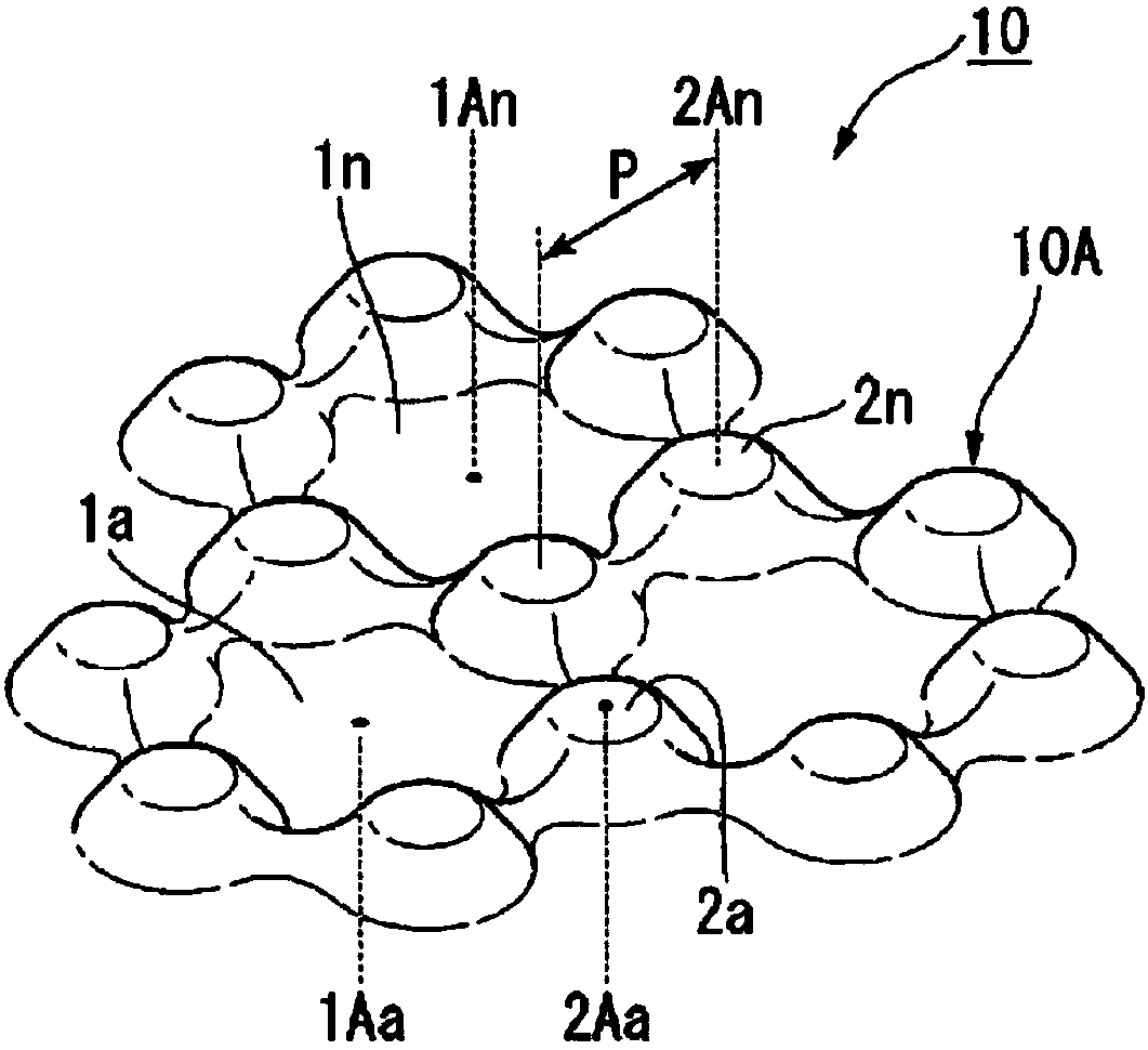
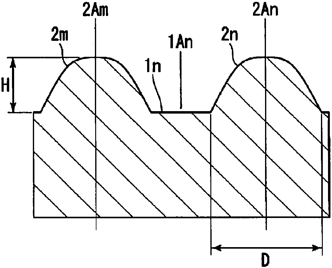
[0052] figure 1 It is a perspective view which schematically shows the mold of one aspect of this invention. In the mold 10 according to one aspect of the present invention, a plurality of flat surfaces 1 a to 1 n and a plurality of convex portions 2 a to 2 n are provided on the main surface 10A. The plurality of flat surfaces 1 a to 1 n are arranged in a region surrounded by the most ...


PUM

PropertyMeasurementUnit
aspect ratioaaaaaaaaaa
thicknessaaaaaaaaaa
aspect ratioaaaaaaaaaa

Abstract

This die has a flat surface and a plurality of projections on the principal surface. The average pitch of the plurality of projections is 50 nm to 5 [mu]m, and the average aspect ratio of the plurality of projections is 0.01 to 1. Eighty percent or more of the plurality of projections have a prescribed curved surface. In the prescribed curved surface, an inclined angle of a second tangent plane incontact with a second point relative to a first tangent plane in contact with a first point is within the range of 60 degrees, where the first point represents any point on the prescribed curved surface and the second point represents a point displaced from the first point by 1 / 10 of the average pitch.

Description

technical field [0001] The invention relates to a mold, a method for manufacturing an organic light emitting diode and the organic light emitting diode. This application claims priority based on Japanese Patent Application No. 2015-178324 for which it applied in Japan on September 10, 2015, and uses the content here. Background technique [0002] Organic light-emitting diodes are light-emitting elements that utilize organic electroluminescence. An organic light emitting diode generally has a structure in which an anode and a cathode are respectively provided on both surfaces of an organic semiconductor layer including a light emitting layer containing an organic light emitting material. The organic semiconductor layer includes an electron injection layer, an electron transport layer, a hole transport layer, a hole injection layer, and the like as necessary, in addition to the light emitting layer. Organic light emitting diodes have advantages such as less viewing angle dep...

Claims


Application Information

Patent Timeline
Patent Type & Authority Applications(China)
IPC IPC(8): H05B33/10B29C33/42B29C59/02H01L51/50H05B33/02
CPCB29C33/42B29C59/02H10K71/00H05B33/02H05B33/10H10K50/00
Inventor 本乡弘毅篠塚启
Owner OJI HLDG CORP
Why Eureka
Try Eureka