Method for reducing irradiation damage based on dislocation

A radiation damage and dislocation technology, applied in electrical components, semiconductor/solid-state device manufacturing, circuits, etc., can solve the problems of uncontrollable dislocation positions, difficulty in introducing dislocations, expensive equipment, etc., to achieve no contamination problems, The effect of huge industrial advantage

Inactive Publication Date: 2018-05-18
INST OF ELECTRONICS ENG CHINA ACAD OF ENG PHYSICS
View PDF2 Cites 4 Cited by
  • Summary
  • Abstract
  • Description
  • Claims
  • Application Information

AI Technical Summary

Problems solved by technology

[0003] At present, the methods of introducing dislocations into silicon mainly include: plastic deformation, which is a relatively common method at present, the introduction of dislocation density is high, but it is destructive, and the position and density of dislocations cannot be controlled; the introduction of oxygen precipitation, this method requires Longer time heat treatment, it is difficult to intro

Method used


Image

  • Method for reducing irradiation damage based on dislocation
  • Method for reducing irradiation damage based on dislocation
  • Method for reducing irradiation damage based on dislocation

Examples


Embodiment 1

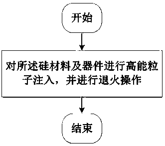
[0025] Taking silicon material as a specific example, a method for reducing radiation damage based on dislocations includes the following steps:

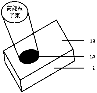
[0026] Such as figure 2 As shown, a single beam of high-energy particles is implanted on the surface of the silicon material 1 , and the high-energy particles in the implanted region 1A are sufficient to destroy the silicon lattice and generate dislocations on the surface of the silicon material 1 . The beam spot diameter of the high-energy particles is 0.1mm to 100mm, and the size of the injection region 1A is controlled by the beam spot of the high-energy particles. As the shape of the beam spot changes, the shape of the injection region 1A changes accordingly. Region 1B that is not implanted with energetic particles will not introduce dislocations.

[0027] High-energy particles include one of protons, neutrons or gamma rays, etc., and the injected dose ranges from 5×10 15 cm -2 up to 5×10 17 cm -2 . The energy range of hi...

Embodiment 2

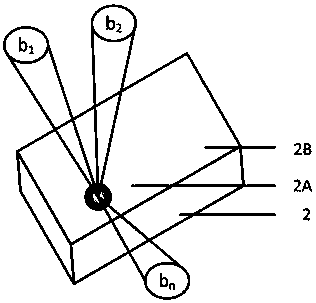
[0029] Such as image 3 As shown, the present invention can also be applied to occasions where it is only necessary to introduce dislocations in the bulk of the silicon material 2 . Multiple beams of high-energy particle beams can be used b 1 , b 2 ... b n Simultaneously implant different surfaces of the silicon material, and adjust the angles between the multiple beams of high-energy particle beams and the respective injection surfaces, so that the multiple beams of high-energy particle beams are focused on a specific area 2A in the silicon material. Under the action of stress, dislocations are introduced in this specific region 2A, while there are few or no dislocations in the region 2B not affected by the convergence of the high-energy particle beam. This method of using multiple high-energy particle beams to introduce dislocations can reduce the power of each high-energy particle beam, effectively reducing its damage to the surface lattice of the silicon material, there...


PUM


Abstract

The invention discloses a method for reducing irradiation damage based on dislocation. The method mainly comprises the following steps of injecting protons, neutrons, gamma rays and other high-energyparticles for a silicon material and a device and carrying out annealing operation, so that the purpose of reducing irradiation damage due to the fact that dislocation with controllable density and controllable position serves as a composite center can be achieved. According to the invention, dislocation is introduced at the specified positions of the silicon material and the device, and dislocation density and dislocation area can be controlled. The dislocation is introduced into the silicon material and the device through irradiation of the high-energy particles to form defects, similar to acomposite center, so that the service life of the carriers is reduced. A large amount of electron-cavity generated in the irradiation process can be compounded by the composite center, so that the number of cavities captured by cavity traps is greatly reduced. Compared with the prior art, the method is advantageous in that for the introduced dislocation, high-energy particles may not affect the electric neutral characteristic of the silicon material and the device, and the irradiation damage of the silicon material and the device is also reduced.

Description

technical field [0001] The invention relates to the technical field of semiconductor manufacturing, in particular to a method for reducing radiation damage based on dislocations. Background technique [0002] When silicon materials and devices continue to work in an ionizing radiation environment, the ionizing radiation will excite electron-hole pairs in the silicon body, and the holes will be captured by hole traps and become fixed space positive charges, resulting in the accumulation of positive charges. When the positive charge accumulates to a certain extent, the leakage current of the device will increase, the electrical characteristic parameters will drift, and eventually fail. [0003] At present, the methods of introducing dislocations into silicon mainly include: plastic deformation, which is a relatively common method at present, the introduction of dislocation density is high, but it is destructive, and the position and density of dislocations cannot be controlled...

Claims


Application Information

Patent Timeline
IPC IPC(8): H01L21/263H01L21/324
Inventor 杨萍董鹏宋宇余学功李沫代刚张健
Owner INST OF ELECTRONICS ENG CHINA ACAD OF ENG PHYSICS
Why Eureka
Try Eureka