
Method for introducing dislocation on silicon chip

A dislocation and silicon wafer technology, applied in electrical components, semiconductor/solid-state device manufacturing, circuits, etc., can solve the problems of harsh thermal care conditions, expensive equipment, and reduced material purity, and is conducive to large-scale industrial production. , The effect of high energy utilization and strong controllability

Inactive Publication Date: 2010-11-10
ZHEJIANG UNIV
View PDF3 Cites 4 Cited by
  • Summary
  • Abstract
  • Description
  • Claims
  • Application Information

AI Technical Summary

Problems solved by technology

[0006] At present, the methods for introducing dislocations into silicon mainly include: 1) Plastic deformation, which is a relatively common method at present, has a high density of introduced dislocations, but it is destructive, and the position and density of dislocations cannot be controlled; 2) Oxygen precipitation 3) Ion implantation (Ion Implantation), the equipment required for this method is relatively expensive, and the subsequent thermal care conditions for the formation of dislocations require Relatively harsh; 4) Wafer Bonding, this method has high production cost, difficult to control dislocation density, and low repeatability; 5) SiGe mismatch, the equipment required for this method is extremely expensive, and heterogeneous materials are introduced, Reduce the purity of the material, and the dislocation density is uncontrollable; 6) Laser irradiation, the dislocation introduced by this method only exists on the surface of the laser irradiation, and cannot be generated inside the material
At the same time, methods 1), 2), and 4) are not compatible with the current integrated circuit technology, and there is a bottleneck problem that is difficult to apply on a large scale

Method used


Image

  • Method for introducing dislocation on silicon chip
  • Method for introducing dislocation on silicon chip
  • Method for introducing dislocation on silicon chip

Examples


Embodiment 1

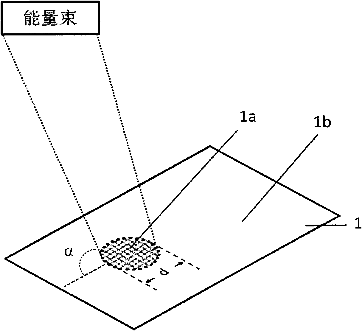
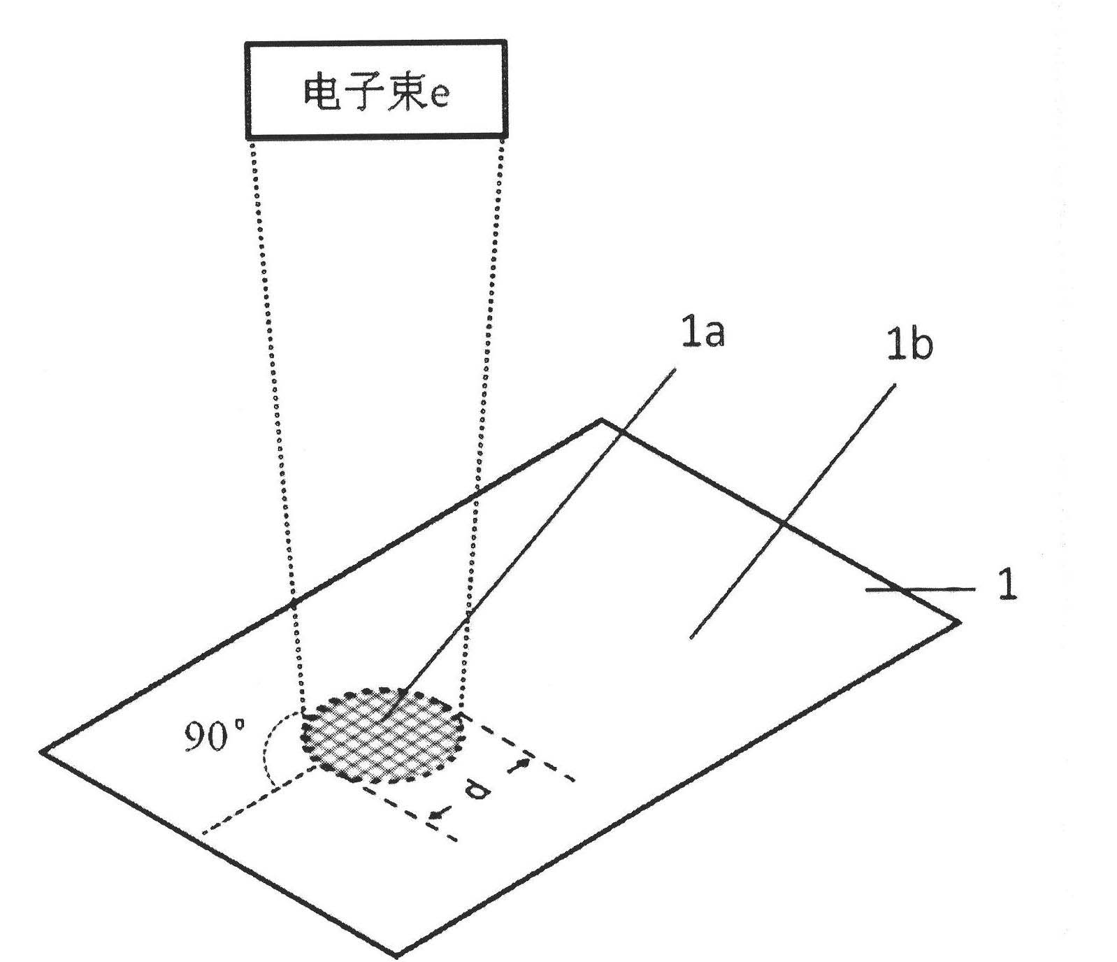
[0035] Such as image 3 As shown, the present embodiment adopts electron beam to p-typeCZ silicon The electron beam is perpendicular to the silicon wafer, the filament voltage in the electron beam evaporation instrument is 82V, the filament current is 0.50A, and the vacuum degree of the back is 5×10 -3 Pa, the beam current of the electron beam is 20mA, the gun voltage is 8.5kV, the beam spot diameter is 6.0mm, and the power per unit area of ​​the electron beam is 1.5W / mm 2 .

[0036] After the irradiation, the irradiated area was a circular area with a diameter of 6mm, and the dislocation density was 5.2×10 6 cm -2 The area with dislocations is consistent with the diameter of the electron beam spot, indicating that the shape of the dislocation area can be controlled by the shape of the electron beam spot.

[0037] With 0.15mol / L of K 2 Cr 4 o 7 The aqueous solution and 50% (mole percent) HF aqueous solution were configured as Secco etching solution at a volume ratio of ...

Embodiment 2

[0040] The experimental conditions of this example are similar to those of Example 1. The n-type CZ silicon wafer is placed at the sample of the electron beam evaporation instrument, the filament voltage is 80V, the filament current is 0.92A, and the vacuum degree of the background is 2×10 -4 Pa, the beam current of the electron beam is 0.9A, the gun voltage is 2.0kV, the beam spot diameter is 4.0mm, and the power per unit area of ​​the electron beam is 458.6W / mm 2 .

[0041] After the irradiation, it was measured that the dislocation density introduced in the irradiated area was 1.2×10 8 cm -2 , and photographed its optical microscopic corrosion topography, such as Figure 7 shown. It can be seen that the present invention can conveniently introduce ultra-high-density dislocations into the silicon wafer by adjusting the energy intensity of the electron beam.

Embodiment 3

[0043] The experimental conditions of this example are similar to those of Example 1. The p-type FZ silicon wafer is placed at the sample of the electron beam evaporation instrument, the filament voltage is 80V, the filament current is 0.60A, and the vacuum degree of the background is 2×10 -2 pa, the beam current of the electron beam is 30mA, the gun voltage is 10.0kV, the beam spot diameter is 1.0mm, and the power per unit area of ​​the electron beam is 382.1W / mm 2 .

[0044] After the irradiation, it was measured that the dislocation density introduced in the irradiated area was 8.1×10 7 cm -2 , and photographed its optical microscopic corrosion topography, such as Figure 8 shown.


PUM


Abstract

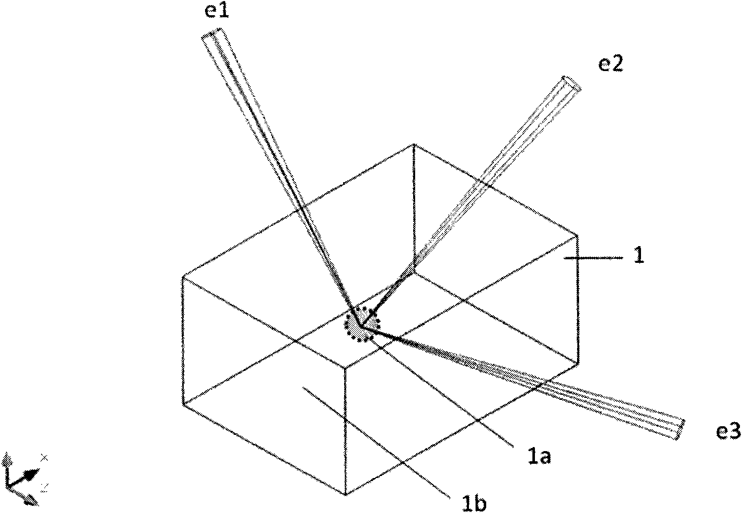
The invention discloses a method for introducing dislocation on a silicon chip. The surface of the silicon chip is radiated by energy beams enough to damage silicon lattices; density-controlled dislocation is introduced into the radiated area; the density of the dislocation is controlled by the intensity of the energy beams, and the density of the introduced dislocation is higher when the energy is stronger; the dislocation can be positioned on the surface of the silicon chip or in the silicon chip; and the energy beams can be electron beams, ion beams, electromagnetic wave beams, alpha X-ray beams, neutron beams or photon beams. The method introduces the controllable dislocation on the silicon chip, is simple and convenient to operate, is well compatible with the conventional integrated circuit process, has the advantages of no damage or contamination to the silicon chip, strong controllability and high repeatability, and is favorable for large-scale industrial production.

Description

technical field [0001] The invention relates to the technical field of semiconductor materials, in particular to a method for introducing dislocations on a silicon wafer. Background technique [0002] As the microelectronics industry represented by integrated circuits continues to develop in the direction of smaller chip sizes, faster processing speeds, and lower costs in accordance with Moore's Law, the integration of devices is getting higher and higher, and the corresponding metal interconnection structures are becoming more and more complex. The degree and length are astonishing. The resulting problems such as interlayer interference, energy dissipation, and signal delay are becoming more and more serious. And the further shrinkage of the feature size will cause the parasitic resistance and capacitance of the planar CMOS to exceed its own channel resistance and capacitance. The rapid development of global optical communication has made the metal interconnection used in...

Claims


Application Information

Patent Timeline
Patent Type & Authority Applications(China)
IPC IPC(8): H01L21/263
Inventor 杨德仁项略略李东升金璐
Owner ZHEJIANG UNIV
Learn More