Infrared, laser and microwave low detectability compatible sub-wavelength structural material

A sub-wavelength structure and laser technology, which is applied in optics, optical components, antennas, etc., can solve the problems of low detectability and mutual compatibility, and achieve the effects of light and thin structure, expanded application range, and simple structure

Active Publication Date: 2018-05-22
INST OF OPTICS & ELECTRONICS - CHINESE ACAD OF SCI
View PDF3 Cites 10 Cited by
  • Summary
  • Abstract
  • Description
  • Claims
  • Application Information

AI Technical Summary

Problems solved by technology

However, there are still some contradictions in achieving mutual compatibility of materials with low detectability in laser, infrared and microwave bands.
The reason is that the microwave band requires strong absorption and low reflection of electromagnetic waves, while the infrared band requires low absorption and high reflection. Although the laser also requires strong absorption and low reflection of electromagnetic waves, it works in the infrared band, which has a low detectability with the infrared band. contradiction

Method used


Image

  • Infrared, laser and microwave low detectability compatible sub-wavelength structural material
  • Infrared, laser and microwave low detectability compatible sub-wavelength structural material
  • Infrared, laser and microwave low detectability compatible sub-wavelength structural material

Examples


Embodiment 1

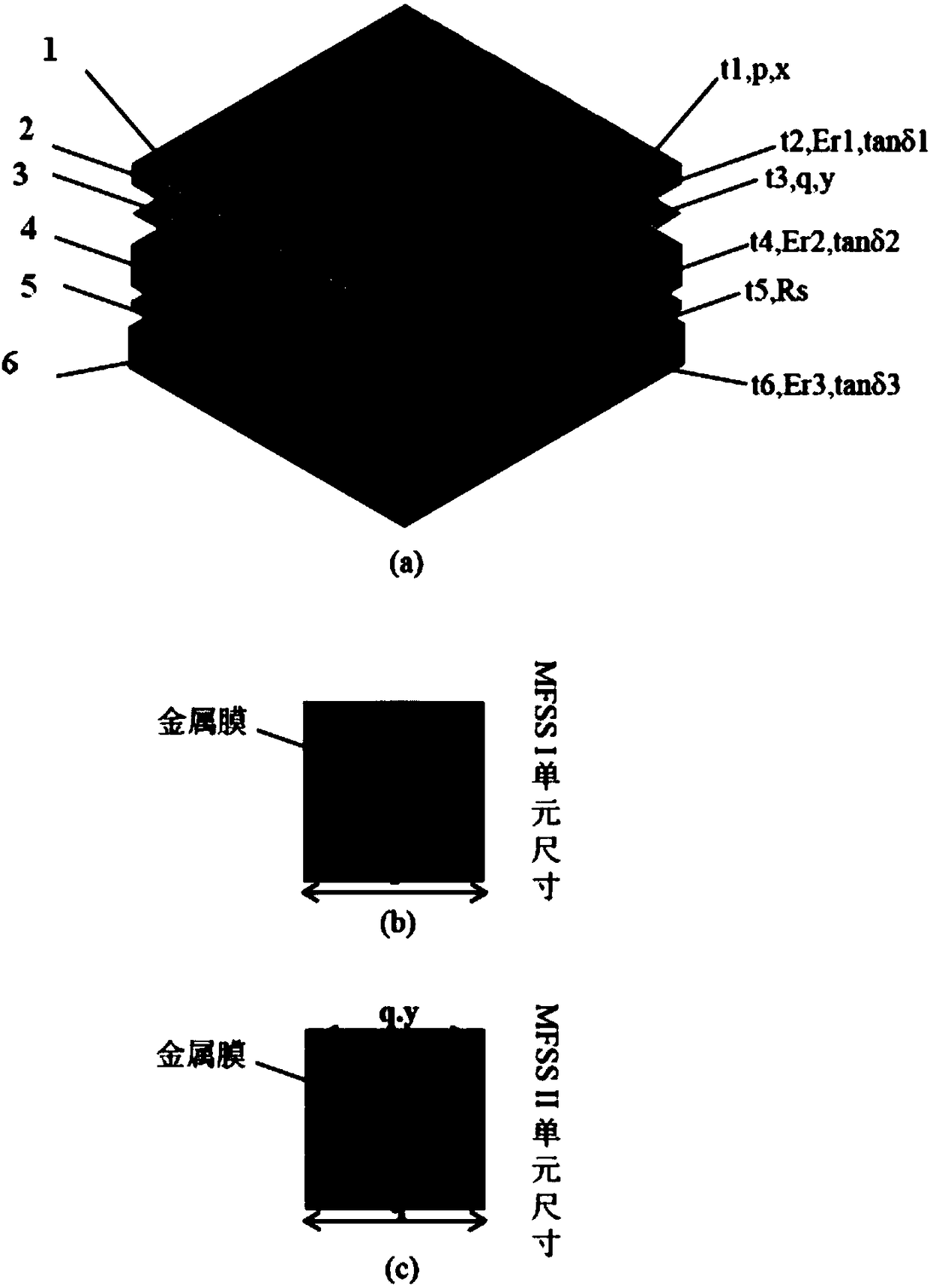
[0022] A sub-wavelength structural material compatible with infrared, laser and microwave low detectability of the present invention, such as figure 1 As shown, the subwavelength structure material sequentially includes a metal-type frequency selective surface layer I, a dielectric layer I, a metal-type frequency selective surface layer II, a dielectric layer II, a resistive film and a dielectric layer III from top to bottom. The specific structural parameter values ​​are shown in Table 2 below.

[0023] Table 2 The structural parameter values ​​of the infrared, laser and microwave low detectability compatible sub-wavelength structural materials of Example 1

[0024]

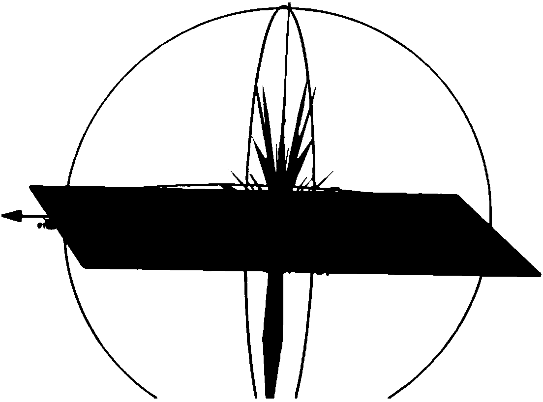
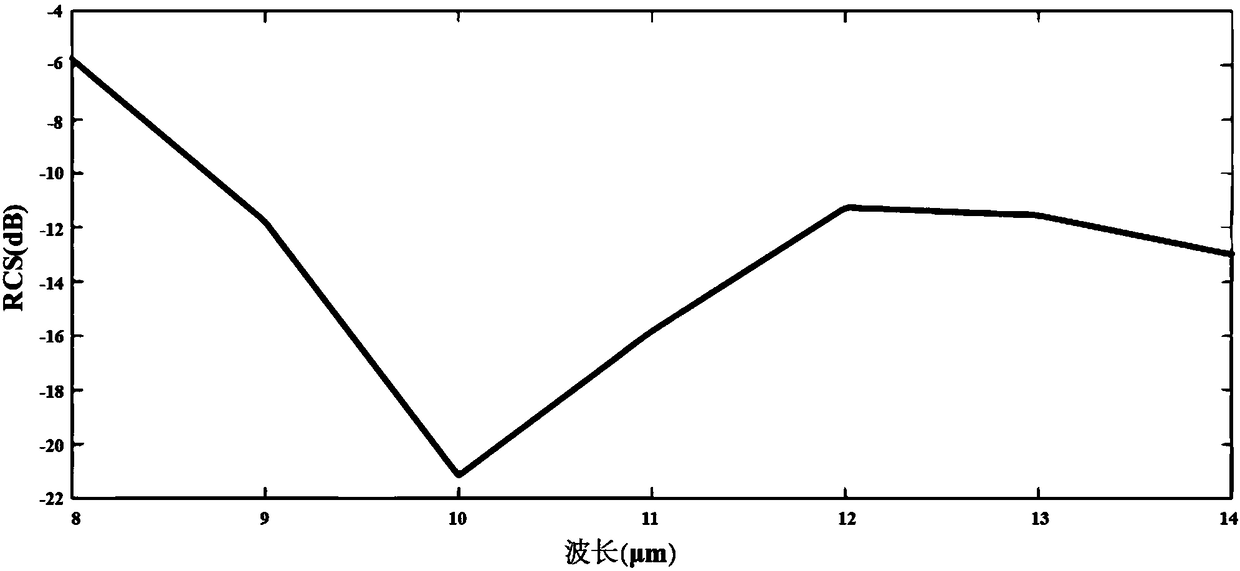
[0025] This embodiment proves the low detectability effect of the present invention on infrared and laser through far-field scattering and RCS reduction, and proves the absorbing effect on microwave through reflectivity. figure 2 It is the far-field scattering diagram of the present invention when the laser...


PUM

PropertyMeasurementUnit
thicknessaaaaaaaaaa
thicknessaaaaaaaaaa
thicknessaaaaaaaaaa

Abstract

The invention discloses an infrared, laser and microwave low detectability compatible sub-wavelength structural material. The infrared, laser and microwave low detectability compatible sub-wavelengthstructural material includes a metal mold frequency selection superficial layer I, a dielectric layer I, a metal mold frequency selection superficial layer II, a dielectric layer II, a resistive filmand a dielectric layer III from top to bottom successively, wherein both the metal mold frequency selection superficial layers are sub-wavelength surface-mounted type arrays, and the used metal has low infrared emitting ability. The infrared, laser and microwave low detectability compatible sub-wavelength structural material utilizes the phase difference generated from two chips with different size on the metal mold frequency selection superficial layer I to regulate the phase so as to control backward scattering of the incident electromagnetic wave to realize low detectability being compatible for laser and infrared, and three layers at the bottom can realize absorption of microwave. The infrared, laser and microwave low detectability compatible sub-wavelength structural material can overcome the limitation that traditional microwave absorbing cladding materials only work in single waveband, can realize compatibility for infrared, laser and microwave, and is simple and light in the material structure.

Description

technical field [0001] The invention relates to the field of multifunctional new materials, in particular to a sub-wavelength structural material compatible with infrared, laser and microwave low detectability. Background technique [0002] With the rapid development of multi-spectral detection technology, the application of single-function absorbing materials can no longer meet the current needs. New absorbing materials compatible with multiple bands, especially laser, infrared and microwave, have become the development direction of research in this field. . However, there are still certain contradictions in achieving mutual compatibility of materials with low detectability in laser, infrared and microwave bands. The reason is that the microwave band requires strong absorption and low reflection of electromagnetic waves, while the infrared band requires low absorption and high reflection. Although the laser also requires strong absorption and low reflection of electromagne...

Claims


Application Information

Patent Timeline
Patent Type & Authority Applications(China)
IPC IPC(8): G02B5/02H01Q17/00
CPCH01Q17/00G02B5/0215G02B5/0284F41H3/00G02B5/003H01Q15/0026G02B1/002G02B5/0294H01Q15/142
Inventor 罗先刚蒲明博李雄马晓亮申国庆
Owner INST OF OPTICS & ELECTRONICS - CHINESE ACAD OF SCI
Why Eureka
Try Eureka