A perovskite solar cell with composite electron transport layer structure
A technology of electron transport layer and solar cell, applied in circuits, electrical components, photovoltaic power generation, etc., can solve problems such as rapid decomposition of perovskite and interface charge recombination, solve interface instability, improve battery performance and stability, high efficiency effect
- Summary
- Abstract
- Description
- Claims
- Application Information
AI Technical Summary
Problems solved by technology
Method used
Image

Examples
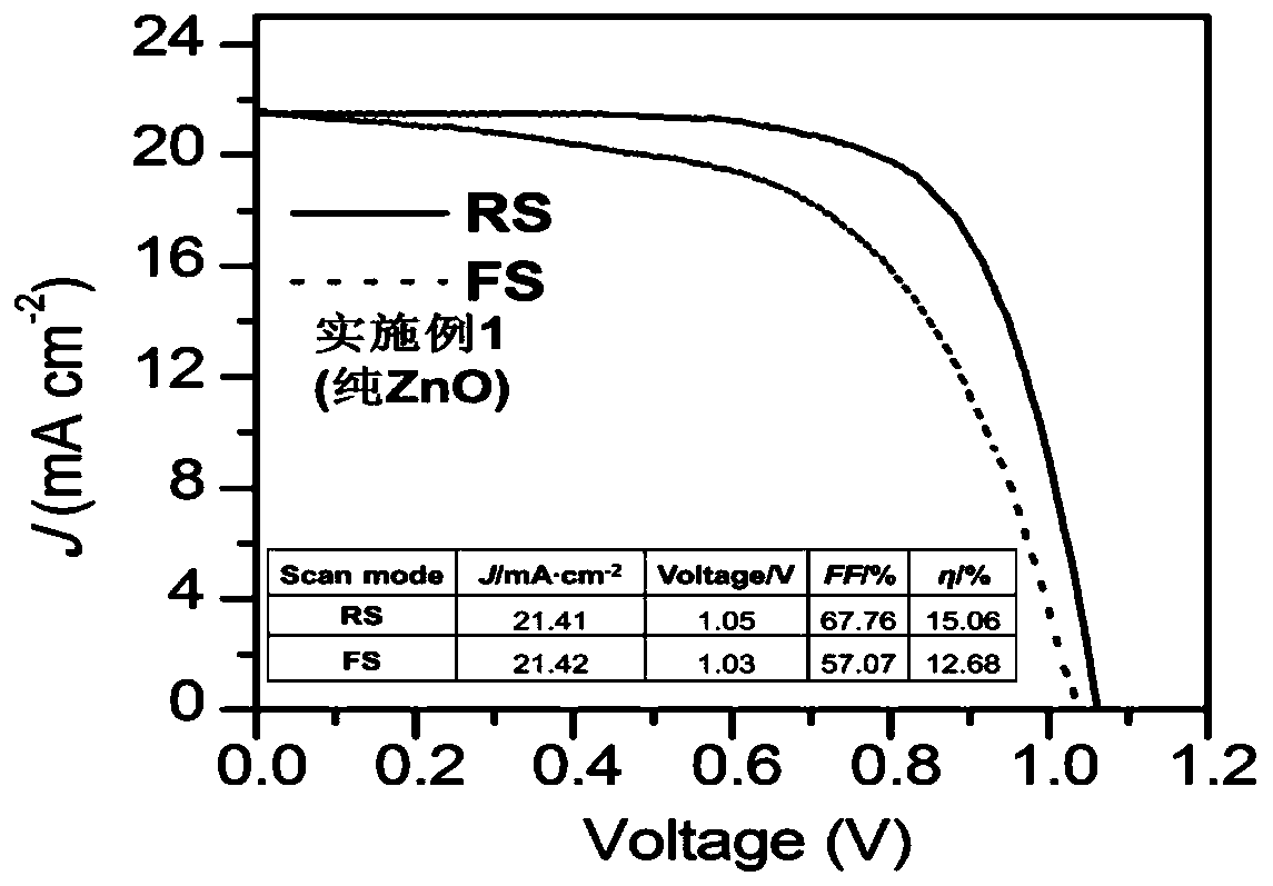
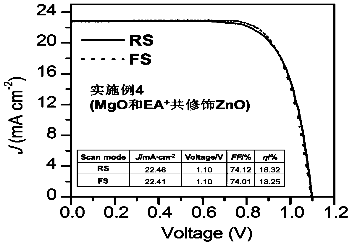
Embodiment 1
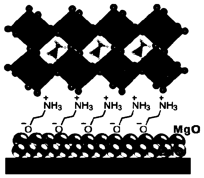
[0028] The perovskite solar cell of the present invention comprises a transparent conductive substrate, a composite electron transport layer, a perovskite absorbing film layer, a hole transport layer and a back electrode stacked in sequence. The perovskite solar cell with this structure can form reasonable energy level matching and conduct charge effectively.
[0029] Preferably, the perovskite film layer of the present invention is MAPbI 3 . MAPbI 3 The thin film has high quality, good energy level matching and low cost.
[0030] Preferably, the hole transport layer material is spiro-OMeTAD. spiro-OMeTAD has a good energy level match with the perovskite film layer, and can effectively transport holes to the back electrode layer, thereby ensuring high photoelectric conversion efficiency.
[0031] The preparation method of this embodiment is:
[0032] The cut 2.0cm×2.0cm transparent conductive substrate FTO was etched with zinc powder and 40mmol / L hydrochloric acid to obta...
Embodiment 2
[0036] The perovskite solar cell of the present invention comprises a transparent conductive substrate, a composite electron transport layer, a perovskite film layer, a hole transport layer and a back electrode stacked in sequence. The perovskite solar cell with this structure can form reasonable energy level matching and conduct charge effectively.
[0037] Preferably, the perovskite film layer of the present invention is MAPbI 3 . MAPbI 3 The thin film has high quality, good energy level matching and low cost.
[0038] Preferably, the hole transport layer material is spiro-OMeTAD. spiro-OMeTAD has a good energy level match with the perovskite film layer, and can effectively transport holes to the back electrode layer, thereby ensuring high photoelectric conversion efficiency.
[0039] The preparation method of this embodiment is:
[0040] The cut 2.0cm×2.0cm transparent conductive substrate FTO was etched with zinc powder and 40mmol / L hydrochloric acid to obtain the des...
Embodiment 3
[0044] The perovskite solar cell of the present invention comprises a transparent conductive substrate, a composite electron transport layer, a perovskite film layer, a hole transport layer and a back electrode stacked in sequence. The perovskite solar cell with this structure can form reasonable energy level matching and conduct charge effectively.
[0045] Preferably, the perovskite film layer of the present invention is MAPbI 3 . MAPbI 3 The thin film has high quality, good energy level matching and low cost.
[0046] Preferably, the hole transport layer material is spiro-OMeTAD. spiro-OMeTAD has a good energy level match with the perovskite film layer, and can effectively transport holes to the gold electrode layer, thereby ensuring high photoelectric conversion efficiency.
[0047] The preparation method of this embodiment is:
[0048] The cut 2.0cm×2.0cm transparent conductive substrate was etched with zinc powder and 40mmol / L hydrochloric acid to obtain the designe...
PUM
| Property | Measurement | Unit |
|---|---|---|
| thickness | aaaaa | aaaaa |
| thickness | aaaaa | aaaaa |
| thickness | aaaaa | aaaaa |
Abstract
Description
Claims
Application Information
 - R&D Engineer
- R&D Manager
- IP Professional
- Industry Leading Data Capabilities
- Powerful AI technology
- Patent DNA Extraction
Browse by: Latest US Patents, China's latest patents, Technical Efficacy Thesaurus, Application Domain, Technology Topic.
© 2024 PatSnap. All rights reserved.Legal|Privacy policy|Modern Slavery Act Transparency Statement|Sitemap