Method, device and equipment for performance test of flash memory chip, and storage medium

A technology of flash memory chips and testing methods, which is applied in the field of memory, can solve problems such as the lack of unified flash memory performance testing process, and achieve the effect of convenient testing

Active Publication Date: 2018-06-08
GIGADEVICE SEMICON (BEIJING) INC
View PDF5 Cites 12 Cited by
  • Summary
  • Abstract
  • Description
  • Claims
  • Application Information

AI Technical Summary

Problems solved by technology

[0004] The present invention provides a performance testing method, device and computer storage medium of a flash memory chip, so as to solve

Method used


Image

  • Method, device and equipment for performance test of flash memory chip, and storage medium
  • Method, device and equipment for performance test of flash memory chip, and storage medium
  • Method, device and equipment for performance test of flash memory chip, and storage medium

Examples


Example Embodiment

[0045] Embodiment one

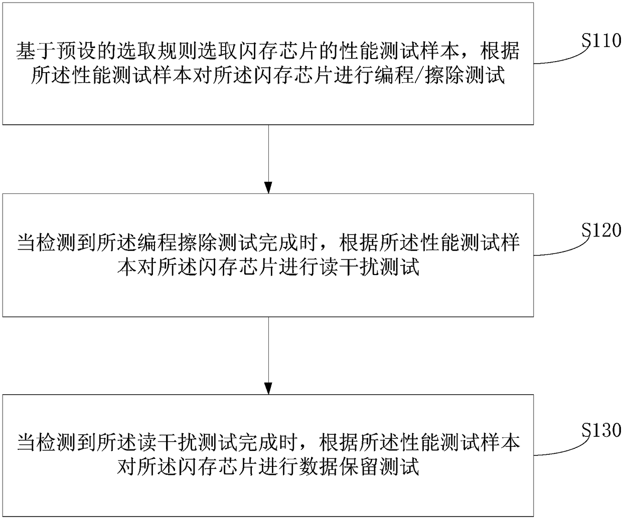
[0046] figure 1 It is a schematic flow chart of a performance testing method of a flash memory chip provided by Embodiment 1 of the present invention. This embodiment is applicable to the performance testing of a flash memory chip. The method can be performed by a performance device of a flash memory chip. and / or in the form of hardware.

[0047] like figure 1 As shown, the method of this embodiment may specifically include:

[0048] S110. Select a performance test sample of the flash memory chip based on a preset selection rule, and perform a programming / erasing test on the flash memory chip according to the performance test sample;

[0049] Wherein, the selection of the performance test samples of the flash memory chip based on the preset selection rules includes: obtaining storage blocks with the same number in each storage wing of the flash memory chip as a set of target storage blocks; obtaining at least two groups of mutually discontinuous numb...

Example Embodiment

[0069] Embodiment two

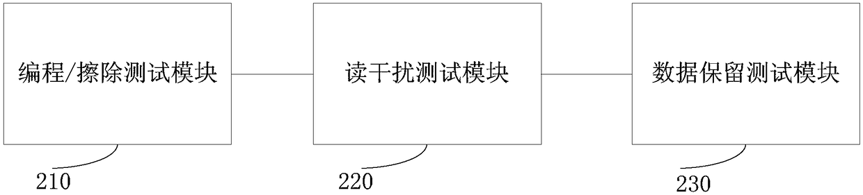
[0070] figure 2 It is a schematic structural diagram of a performance testing device for a flash memory chip provided by Embodiment 2 of the present invention, and the device includes: a programming / erasing testing module 210 , a read disturbance testing module 220 and a data retention testing module 220 .

[0071] Wherein, the programming / erasing test module 210 is used to select performance test samples of flash memory chips based on preset selection rules, and perform programming / erasing tests on the flash memory chips according to the performance test samples; read disturbance test module 220, For when it is detected that the programming / erasing test is completed, perform a read disturbance test on the flash memory chip according to the performance test sample; the data retention test module 220 is used for when it is detected that the read disturbance test is completed, performing a data retention test on the flash memory chip according to the pe...

Example Embodiment

[0079] Embodiment three

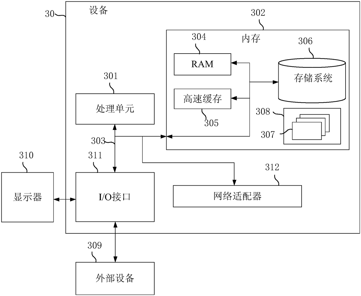
[0080] image 3 It is a schematic structural diagram of a device provided by Embodiment 3 of the present invention. image 3 A block diagram of an exemplary apparatus 30 suitable for implementing embodiments of the invention is shown. image 3The shown device 30 is only an example, and should not impose any limitation on the functions and scope of use of the embodiments of the present invention.

[0081] like image 3 As shown, device 30 takes the form of a general purpose computing device. Components of the device 30 may include, but are not limited to: one or more processors or processing units 301 , a system memory 302 , and a bus 303 connecting different system components (including the system memory 302 and the processing unit 301 ).

[0082] Bus 303 represents one or more of several types of bus structures, including a memory bus or memory controller, a peripheral bus, an accelerated graphics port, a processor, or a local bus using any of a ...


PUM


Abstract

The invention discloses a method, a device and equipment for a performance test of a flash memory chip and a storage medium. The method comprises the steps of selecting a performance test sample of the flash memory chip based on a preset selection rule, and performing a programming/erasing test on the flash memory chip according to the performance test sample; when detecting that the programming/erasing test is completed, performing a read interference test on the flash memory chip according to the performance test sample; and when detecting that the read interference test is completed, performing a data retention test on the flash memory chip according to the performance test sample. With the technical scheme of the embodiment, the problem in the prior art of no unified flash memory performance test flow is solved and the effect of the flash memory performance test is achieved conveniently and rapidly.

Description

technical field [0001] The embodiments of the present invention relate to the technical field of memory, and in particular, to a performance testing method, device and computer storage medium of a flash memory chip. Background technique [0002] Nand Flash is increasingly favored by the storage industry because of its large capacity and fast rewriting speed. The internal structure of storage devices commonly used in the market, such as U disks and SSDs, is composed of Nand Flash flash memory particles and controllers. The firmware in the controller should be closely related to the flash memory particles used during the development process. [0003] When developing chips based on flash memory particles, the first process is usually to test some basic functions and characteristics of flash memory particles, so as to make some targeted measures in the firmware development project. The research on Nand Flash needs to understand the influence of each parameter, and at the same ...

Claims


Application Information

Patent Timeline
IPC IPC(8): G11C29/56
CPCG11C29/56
Inventor 刘凯
Owner GIGADEVICE SEMICON (BEIJING) INC
Why Eureka
Try Eureka