Photoelectric detector, manufacturing method thereof and photoelectric detector fabric

A technology for photodetectors and manufacturing methods, which is applied in photovoltaic power generation, electric solid-state devices, semiconductor/solid-state device manufacturing, etc. It can solve problems such as low sensitivity, loss of detection optical signals, and single frequency band of detection light waves, so as to improve the output photocurrent , Increase light transmittance, improve the effect of carrier transport

Inactive Publication Date: 2018-06-12
SHANGHAI INTEGRATED CIRCUIT RES & DEV CENT
View PDF2 Cites 7 Cited by
  • Summary
  • Abstract
  • Description
  • Claims
  • Application Information

AI Technical Summary

Problems solved by technology

Among them, photodetectors, as representative sensors, have important applications in medical treatment, detection, military and other fields, but traditional photodetectors are mostly block-shaped and hard plate-shaped devices, which are difficult to fit irregular substrates according to application requirements, and do not have Flexible and bendable characteristics, these problems severely limit its development in wearable devices and other related fields
In addition, photodetectors sensitive to near-infrared or infrared still have problems such as serious loss of detection light signal, single frequency band of detection light wave, low sensitivity and insufficient flexibility of devices.

Method used


Image

  • Photoelectric detector, manufacturing method thereof and photoelectric detector fabric
  • Photoelectric detector, manufacturing method thereof and photoelectric detector fabric
  • Photoelectric detector, manufacturing method thereof and photoelectric detector fabric

Examples


Embodiment Construction

[0026] In order to make the objects, features and advantages of the present invention more comprehensible, please refer to the accompanying drawings. It should be noted that the structures, proportions, sizes, etc. shown in the drawings attached to this specification are only used to match the content disclosed in the specification, for those who are familiar with this technology to understand and read, and are not used to limit the implementation of the present invention. Limiting conditions, so there is no technical substantive meaning, any modification of structure, change of proportional relationship or adjustment of size, without affecting the effect and purpose of the present invention, should still fall within the scope of the present invention. within the scope covered by the disclosed technical content.

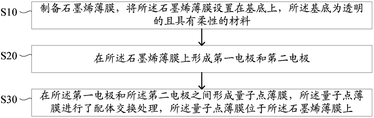
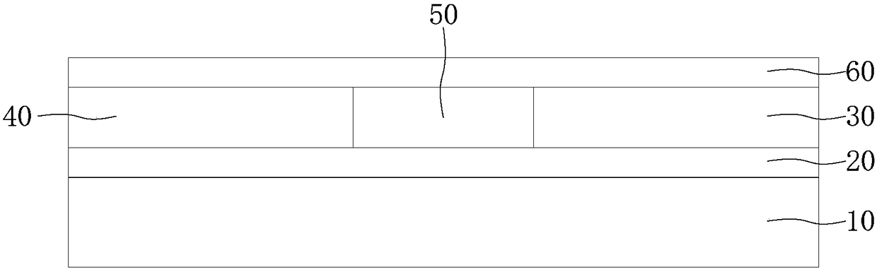
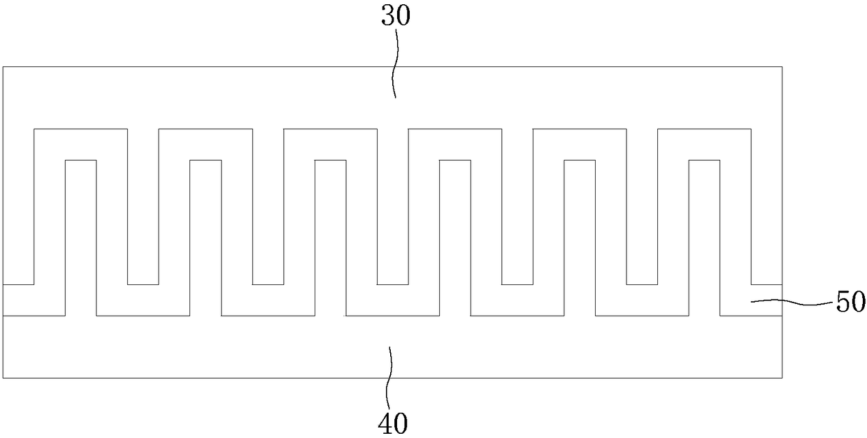
[0027] Such as figure 1 As shown, the present invention provides a kind of fabrication method of photodetector, the fabrication method of described photodetector co...


PUM

PropertyMeasurementUnit
widthaaaaaaaaaa
band gapaaaaaaaaaa
thicknessaaaaaaaaaa

Abstract

The invention provides a photoelectric detector, a manufacturing method thereof and photoelectric detector fabric. The manufacturing method of the photoelectric detector comprises the steps of preparing graphene thin film and arranging the graphene thin film on a substrate, wherein the substrate is made of a light-transmitting and flexible material; forming a first electrode and a second electrodeon the graphene thin film; forming quantum point thin film between the first electrode and the second electrode, wherein the quantum point thin film is subjected to ligand exchange treatment. By means of the photoelectric detector, the manufacturing method thereof and the photoelectric detector fabric, the quantum point thin film is located on the graphene thin film, carriers generated by an illumination response of the quantum point thin film can be transmitted by graphene, and the carrier transmitting performance of a photosensitive layer quantum point is improved; meanwhile, the photoelectric detector is arranged on the light-transmitting graphene thin film, based on the light-transmitting and flexible substrate, the light transmittance is increased, and thus the photoelectric detectorhas flexibility, bending performance and a weaving capability.

Description

technical field [0001] The invention relates to the field of semiconductor manufacturing, in particular to a photodetector, a manufacturing method thereof, and a photodetector fabric. Background technique [0002] In recent years, the vigorous development of wearable electronic devices has promoted technological progress in many fields, such as display, sensors, energy harvesting and storage, and the lightness, flexibility and bendability of wearable devices have attracted widespread attention. Among them, photodetectors, as representative sensors, have important applications in medical treatment, detection, military and other fields, but traditional photodetectors are mostly block-shaped and hard plate-shaped devices, which are difficult to fit irregular substrates according to application requirements, and do not have Flexible and bendable, these problems severely limit its development in wearable devices and other related fields. In addition, photodetectors sensitive to ...

Claims


Application Information

Patent Timeline
Patent Type & Authority Applications(China)
IPC IPC(8): H01L51/48H01L51/42
CPCH10K71/12H10K30/00Y02E10/549Y02P70/50
Inventor 武青青胡少坚朱建军
Owner SHANGHAI INTEGRATED CIRCUIT RES & DEV CENT
Why Eureka
Try Eureka