

Mount structure
A technology of structure and crystal structure, which is applied in the manufacture of electrical solid devices, semiconductor devices, semiconductor/solid devices, etc., can solve the problems of large thermal stress, cracks, large joint area, etc., and suppress the occurrence and development of cracks , the effect of large thermal stress
- Summary
- Abstract
- Description
- Claims
- Application Information
AI Technical Summary
Problems solved by technology
Method used
Image

Examples
Embodiment
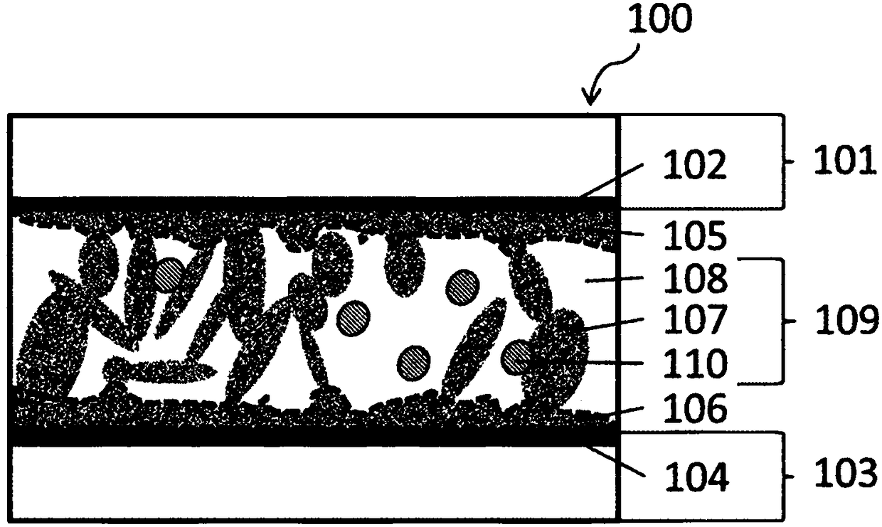
[0054] In order to confirm the effect of the present invention, regarding the above-mentioned embodiment, a 10mm 2 、15mm 2 The large-area bonded installation structure is verified. Here, as the first member 101, a 15mm steel plate with Ni plating on the back as the first material to be joined 102 is used. 2 Si chips. In addition, as the second member 103 , a Cu plate having Ni plating as the second material to be joined 104 on the back was used. The installation structure is manufactured according to the following steps.
[0055] First, flux is applied to a Cu plate as the second member 103, and a foil of a solder material forming the bonding material layer 109 is supplied thereon. In addition, flux is applied to the foil of the solder material, and the Si chip as the first member 101 is mounted thereon. It is heated to 280°C to melt the solder material. In the melted state, pressing is performed by applying a downward force from above the Si chip, and the layer thicknes...
Embodiment 3
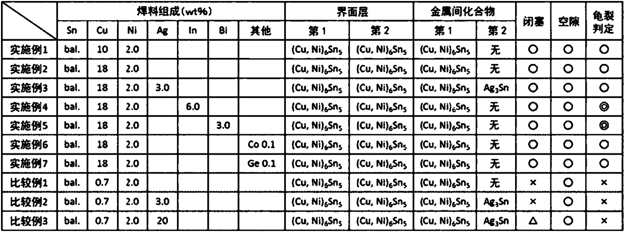
[0062] The Ag contained in the solder materials of Example 3 and Comparative Example 2 was equal to the Ag content of the second intermetallic compound 110. 3 Sn exists in the form of Sn and is dispersed in the bonding material layer 109 .
[0063] On the other hand, in Comparative Examples 1 and 2, the content of Cu was small, so the (Cu, Ni) of the first intermetallic compound 107 6 sn 5 Less, unable to confirm occlusion. In addition, in Comparative Example 3, the content of Ag is large, so Ag 3 A large amount of Sn exists in the form of the second intermetallic compound 110 to form a closed structure.
[0064] In addition, elements other than Cu and Ni contained in the welding materials of Examples 4 to 7 do not exist in the form of the first intermetallic compound 107, and In and Bi are solid-dissolved in the stress relaxation material 108, and Co and Ge are trace amounts. Although not observed, it is considered to be contained in any one of the first interface layer 1...
PUM
 Abstract
Description
Claims
Application Information