Semiconductor package with a support structure and fabrication method thereof

Active Publication Date: 2007-03-15
SILICONWARE PRECISION IND CO LTD
View PDF5 Cites 33 Cited by
  • Summary
  • Abstract
  • Description
  • Claims
  • Application Information

AI Technical Summary

Benefits of technology

[0015] Therefore, according to the semiconductor package with a support structure and the fabrication method thereof in the present invention, after the chip is electrically connected to the electrical contacts of the semiconductor package, the molding process is performed and the recessed portions formed on the carrier are filled with the encapsulant for encapsulating the chip when the encapsulant is injected. As a result, when the carrier is removed, the part of the encapsulant filling the recessed portions forms the protruded portions on the surface of the encapsulant, such that the semiconductor package can be attached to an external device via the protruded portions. Thereby, unlike the prior art, the present invention avo

Problems solved by technology

However, the thickness of the lead-frame-based semiconductor package cannot be further reduced as having to count the thickness of the lead frame.
During the fabrication processes, thermal stress may be produced between the package and the printed circuit board due to mismatch in Coefficient of Thermal Expansion (CTE) between materials of the package and the printed circuit board.
As the foregoing package is bonded to the printed circuit board by SMT and through the solder joints only, due to the CTE mismatch between the package and the printed circuit board, significant thermal stress is exerted to the solder joints.
In the foregoing package, the solder joints 3

Method used


Image

  • Semiconductor package with a support structure and fabrication method thereof
  • Semiconductor package with a support structure and fabrication method thereof
  • Semiconductor package with a support structure and fabrication method thereof

Examples


Example

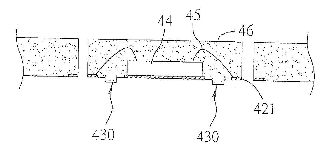
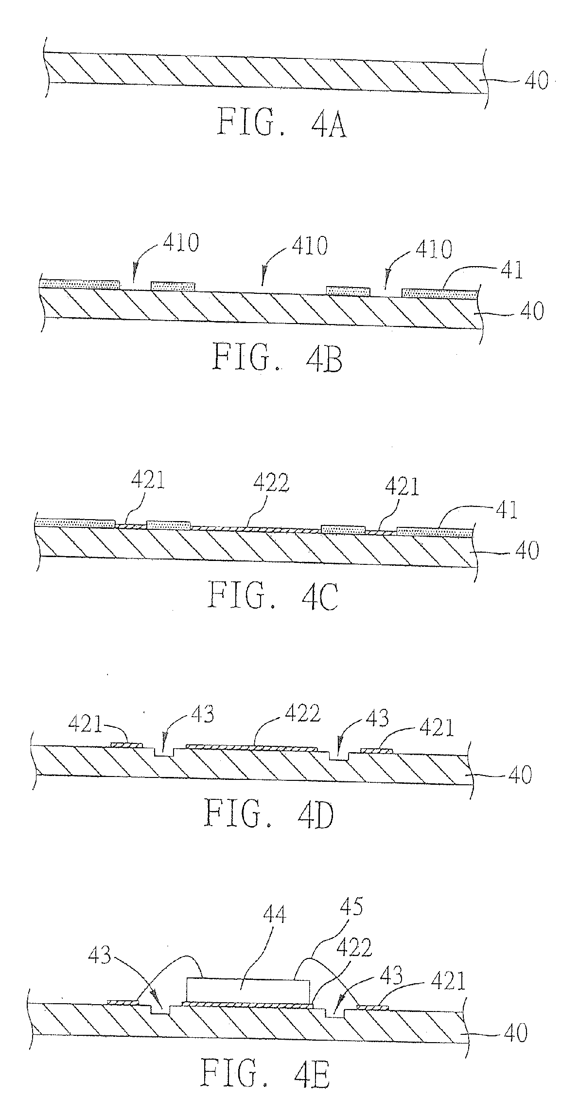
[0027] Preferred embodiments of a semiconductor package with a support structure and a fabrication method thereof proposed in the present invention are described as follows with reference to FIGS. 4 to 10.

[0028]FIGS. 4A to 4G are cross-sectional views showing steps of the fabrication method of a semiconductor package with a support structure according to a preferred embodiment of the present invention. It should be noted that the drawings are schematic diagrams showing the basic components relating to the present invention, and the present invention is not particularly limited to the type, number, shape and size of the components shown in the drawings, that is, the arrangement of components may be more complicated in practical implementation.

[0029] As shown in FIG. 4A, firstly, a carrier 40 is prepared, which is made of a metal material such as copper and serves as a conductive path for a plating current used in a subsequent electroplating process.

[0030] Next, as shown in FIG. 4B...


PUM


Abstract

A semiconductor package with a support structure and a fabrication method thereof are provided. With a chip being electrically connected to electrical contacts formed on a carrier, a molding process is performed. A plurality of recessed portions formed on the carrier are filled with an encapsulant for encapsulating the chip during the molding process. After the carrier is removed, the part of the encapsulant filling the recessed portions forms outwardly protruded portions on a surface of the encapsulant, such that the semiconductor package can be attached to an external device via the protruded portions.

Description

FIELD OF THE INVENTION [0001] The present invention relates to semiconductor packages and fabrication methods thereof, and more particularly, to a semiconductor package with a support structure and a fabrication method of the semiconductor package. BACKGROUND OF THE INVENTION [0002] A lead frame is usually used as a chip carrier for mounting a semiconductor chip thereon to form a semiconductor package. The lead frame comprises a die pad and a plurality of leads around the die pad. After the semiconductor chip is attached to the die pad and is electrically connected to the leads by bonding wires, an encapsulant is formed to encapsulate the chip, the die pad, the bonding wires and inner portions of the leads, thereby completing the semiconductor package. [0003] Various types of lead-frame-based semiconductor packages have been developed such as QFP (Quad Flat Package), QFN (Quad Flat Non-leaded) package, SOP (Small Outline Package), DIP (Dual in-line Package) and so on. In order to im...

Claims


Application Information

Patent Timeline
IPC IPC(8): H01L21/00
CPCH01L21/561H01L21/568H01L2224/48247H01L2924/1815H01L2224/16245H01L2924/014H01L2924/01033H01L2924/01082H01L24/97H01L2224/48091H01L2224/49171H01L2224/97H01L2924/01027H01L2924/01029H01L2924/01046H01L2924/01078H01L2924/01079H01L2924/00014H01L2224/85H01L2924/00H01L2924/15747H01L2924/181H01L2924/351H01L2924/00012
Inventor HUANG, CHIEN-PINGTANG, FU-DI
Owner SILICONWARE PRECISION IND CO LTD
Why Eureka
Try Eureka