A kind of ultra-thin oled screen body and its manufacturing process

An ultra-thin, isolation belt technology, used in semiconductor devices, electrical solid-state devices, electrical components, etc., can solve the problems of poor screen reliability, overflowing glue, and difficult screen cutting, so as to improve product yield and improve product quality. High rate, easy to achieve effect

Active Publication Date: 2020-09-22
GUAN YEOLIGHT TECH CO LTD
View PDF4 Cites 0 Cited by
  • Summary
  • Abstract
  • Description
  • Claims
  • Application Information

AI Technical Summary

Problems solved by technology

Although the above-mentioned packaging solutions are mature in technology, low in cost, and widely used, the widening of UV glue cannot be accurately controlled, and the adverse consequences include: if the amount of UV glue is too small, the reliability of the screen will be poor; If the amount of UV glue is too large, it will cause glue overflow
And once the glue overflows, if it overflows into the light-emitting area, the UV glue will affect the luminescent material; if it overflows into the lead section of the screen, the UV glue will cause difficulty in cutting the screen and poor appearance of the screen, which needs to be improved urgently

Method used


Image

  • A kind of ultra-thin oled screen body and its manufacturing process
  • A kind of ultra-thin oled screen body and its manufacturing process
  • A kind of ultra-thin oled screen body and its manufacturing process

Examples


Embodiment 1

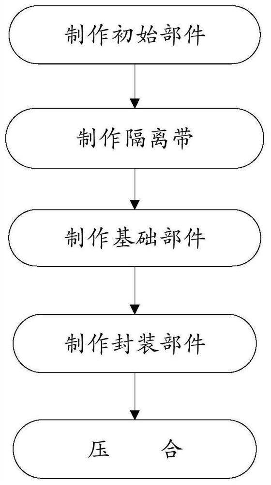
[0034] Please refer to figure 1 A disclosed manufacturing process of an ultra-thin OLED screen comprises the following steps:

[0035] Making the initial component: forming the first electrode on the substrate;

[0036] Making isolation strips: forming two parallel isolation strips on the substrate and the two isolation strips are distributed along the circumference of the substrate;

[0037] Making the basic components: forming a light-emitting layer on the first electrode, and forming a second electrode on the light-emitting layer;

[0038] Making packaging components: making a dispensing pattern along the circumference of the packaging cover plate and the dispensing pattern corresponds to the isolation belt pattern;

[0039] Pressing: Pressing the base part and the package part, so that the dispensing pattern on the package cover can be between the two isolation strips.

[0040] In the above manufacturing process steps, making initial components is a basic step.

[0041...

Embodiment 2

[0051] The difference from Embodiment 1 is that in the step of making the initial component, it also includes forming a metal auxiliary electrode on the first electrode through a photolithography process, and forming an insulating layer such as Figure 5As shown, the isolation zone and the insulating layer are prepared on the same layer.

[0052] In any preferred embodiment, the isolation zone and the insulating layer have the same material and are prepared on the same layer by a photolithography process.

[0053] In this embodiment, the metal auxiliary electrode is formed on the first electrode, and is patterned by a photolithography process, and then spin-coats PI photoresist on the entire surface of the substrate, and exposes and develops according to a predetermined pattern to obtain an insulating layer Graphics and Barrier Graphics.

[0054] In this embodiment, the metal auxiliary electrode is selected from but not limited to Mo / Al / Mo, Cr / Al / Cr, and the insulating layer ...

Embodiment 3

[0059] The difference from Embodiment 2 is that in the step of making the initial component, it also includes forming a metal auxiliary electrode on the first electrode through a photolithography process, forming an insulating layer on the metal auxiliary electrode through a photolithography process, and forming an isolation layer on the insulating layer. Zhuru Image 6 As shown, the isolation zone is prepared on the same layer as the isolation column.

[0060] The isolation column is prepared on the insulating layer and has an inverted trapezoidal structure, and the material of the isolation column is selected from but not limited to PI photoresist.

[0061] In this embodiment, the isolation strip and the isolation column are prepared on the same layer, and both are inverted trapezoidal structures, and both have the same shape, which greatly saves the process.

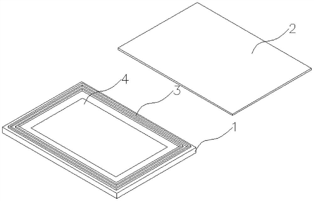
[0062] The structure of an ultra-thin OLED panel obtained according to Embodiment 1, 2 or 3 is as follows.


PUM


Abstract

This application provides an ultra-thin OLED screen body and its manufacturing process. Based on the technical solution in this application, the specific structure of the ultra-thin OLED screen body provided by this application can utilize the existence of two parallel isolation strips to limit the The widening area of ​​glue dispensing effectively solves the problem of glue overflow in the prior art and improves the product yield; based on the above technical solution, the manufacturing process of the ultra-thin OLED screen body provided by this application is better than that of the prior art , The isolation strip is prepared on the same layer as the insulating layer or the isolation column, which greatly simplifies the process steps and improves the production efficiency.

Description

technical field [0001] The present disclosure generally relates to the technical field of electronic display, and in particular relates to an ultra-thin OLED screen body and a manufacturing process thereof. Background technique [0002] OLED (Organic Light Emitting Display, Chinese name Organic Light Emitting Display) refers to the phenomenon that organic semiconductor materials and luminescent materials are driven by an electric field to cause light emission through carrier injection and recombination. Displays or lighting products made according to this light-emitting principle are called organic light-emitting displays or organic light-emitting lighting products. Flexibility, bending, and ultra-thinness have become the future development direction of OLED screens, and packaging technology will be an important factor restricting its development. [0003] At present, the packaging method in the common packaging technology of OLED ultra-thin products is: using UV glue and f...

Claims


Application Information

Patent Timeline
Patent Type & Authority Patents(China)
IPC IPC(8): H01L27/32
CPCH10K59/88
Inventor 董艳波陈旭张国辉谢静吕勇鲁天星王国健
Owner GUAN YEOLIGHT TECH CO LTD
Why Eureka
Try Eureka