
A column readout circuit applied to cmos image sensor

An image sensor and column readout technology, which is applied in image communication, television, electrical components, etc., can solve the problem of limited frame rate, limited single-ended structure column readout circuit, difficulty in realizing wide dynamic range and high frame rate characteristics, etc. problem, to achieve the effect of increasing speed, increasing the maximum output voltage range, and improving the dynamic range

Active Publication Date: 2019-09-20
ZHEJIANG UNIV
View PDF2 Cites 0 Cited by
  • Summary
  • Abstract
  • Description
  • Claims
  • Application Information

AI Technical Summary

Problems solved by technology

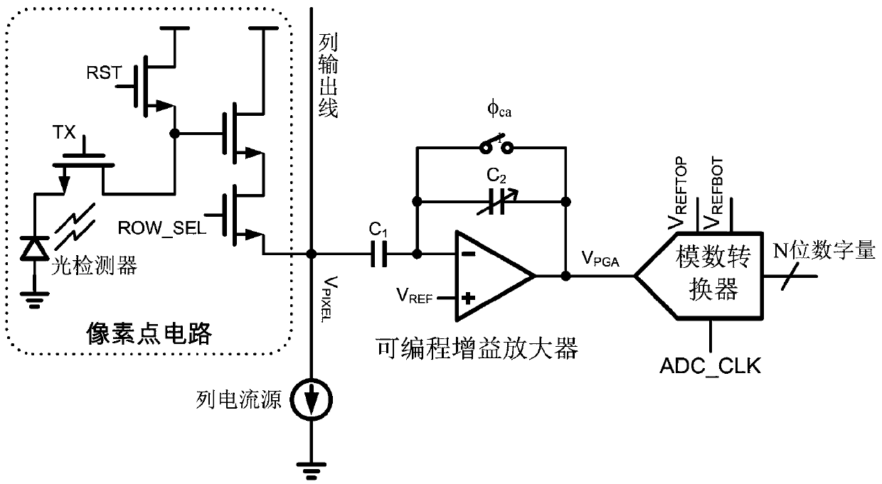
(3) The analog-to-digital converter converts the analog output voltage of the programmable gain amplifier into a digital quantity twice successively, and finds the difference between the two to provide to the imaging device. Each pixel signal sampling requires two analog-to-digital conversions Converter transition time, limiting the overall frame rate
To sum up, the single-ended structure column readout circuit is limited by the structure itself, and it is difficult to achieve wide dynamic range and high frame rate characteristics

Method used


Image

  • A column readout circuit applied to cmos image sensor
  • A column readout circuit applied to cmos image sensor
  • A column readout circuit applied to cmos image sensor

Examples


Embodiment Construction

[0025] In order to describe the present invention more specifically, the technical solutions of the present invention will be described in detail below in conjunction with the accompanying drawings and specific embodiments.

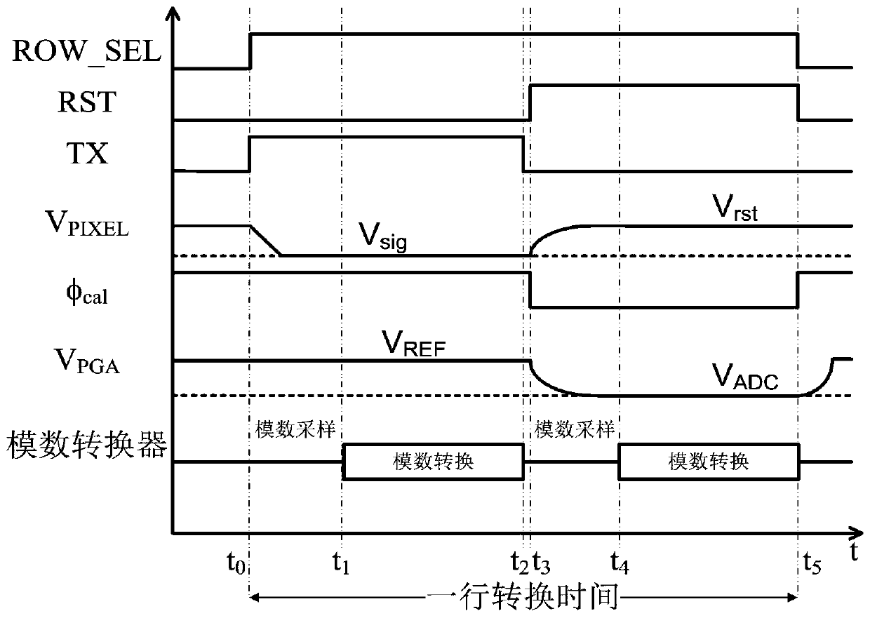
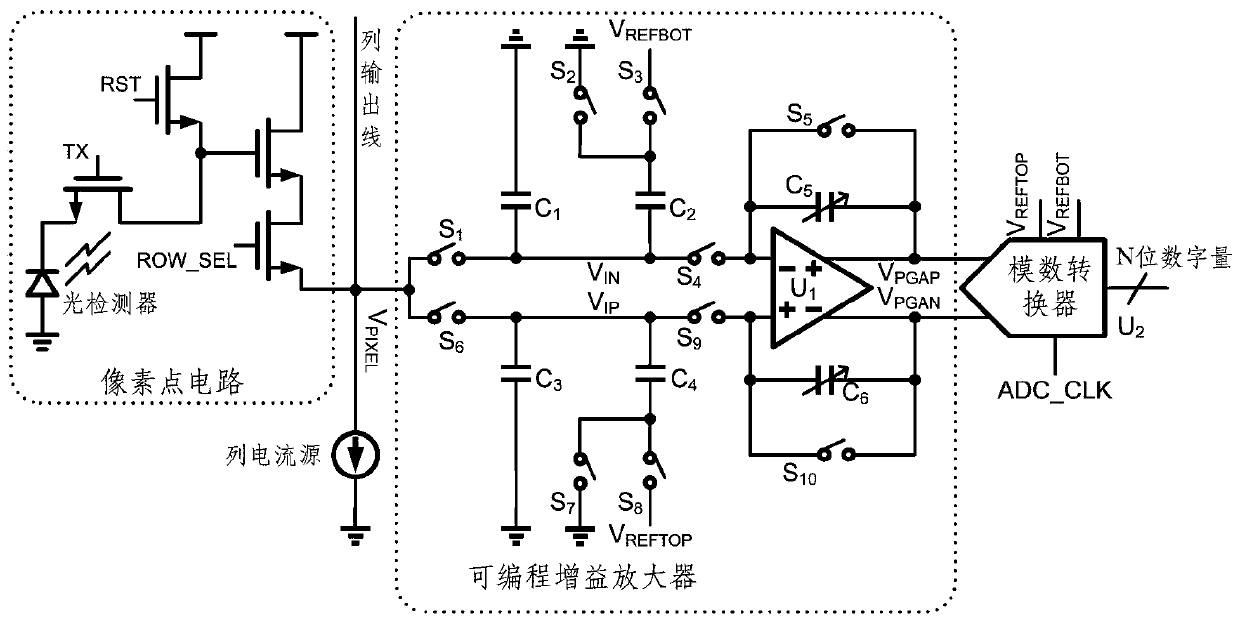
[0026] The column readout circuit of the present invention constitutes as image 3 shown by the programmable gain amplifier sampling capacitor C 1 、C 2 、C 3 、C 4 with variable amplification capacitor C 5 、C 6 , fully differential amplifier U 1 with a successive approximation ADC U 2 composition. The key timing waveforms of the readout circuit are as Figure 4 As shown in FIG. 1 , within the conversion time of one line, the single-ended signal output by the pixel point circuit is sampled time-divisionally and block-by-block by the sampling capacitor of the programmable gain amplifier. During the exposure phase, V sig signal and V REFBOT The reference signal is sampled to the side sampling capacitor C 1 、C 2 ; while in the reset phase, V rst s...


PUM


Abstract

The invention discloses a column readout circuit applied to a CMOS image sensor, which comprises a programmable gain amplifier for converting a single-end unipolar signal to a double-end bipolar signal and a differential input two-step successive approximation analog-to-digital converter. The circuit uses a programmable gain amplifier with time-division and block sampling and switched capacitor level shifting technology to convert the pixel output voltage into a double-ended bipolar signal with a larger amplitude to improve the dynamic range of the signal; The stepwise successive approximation analog-to-digital converter converts the double-terminal bipolar analog signal output by the programmable amplifier into a digital signal, which is provided to the imaging device. Therefore, the column readout circuit of the present invention is applied to a CMOS image sensor, which can realize the characteristics of large dynamic range and high frame rate.

Description

technical field [0001] The invention belongs to the technical field of integrated circuit design, and in particular relates to a column readout circuit applied to a CMOS image sensor. Background technique [0002] With the continuous development of CMOS technology, the application range of CMOS image sensors is becoming more and more extensive because of its low power consumption, simple power supply, high integration, and low cost. With the continuous improvement of imaging quality requirements, the number of pixels and frame frequency of image sensors continue to increase, and higher requirements are placed on the accuracy and speed of the matching readout circuit. Therefore, it is important to improve the dynamic range and conversion frequency of the readout circuit. Technical problems that image sensor technology must solve. Under the existing technical conditions, the readout circuit is divided into a global readout circuit, a column readout circuit and a pixel point r...

Claims


Application Information

Patent Timeline
Patent Type & Authority Patents(China)
IPC IPC(8): H04N5/374H04N5/378H04N5/355
CPCH04N25/57H04N25/76H04N25/75
Inventor 李浙鲁何乐年奚剑雄
Owner ZHEJIANG UNIV
Learn More