Bonding alignment precision detection method and semiconductor device

A detection method and technology of alignment accuracy, applied in the direction of semiconductor devices, semiconductor/solid-state device parts, semiconductor/solid-state device testing/measurement, etc. drop etc.

Active Publication Date: 2018-06-26
SEMICON MFG INT (SHANGHAI) CORP +1
View PDF3 Cites 11 Cited by
  • Summary
  • Abstract
  • Description
  • Claims
  • Application Information

AI Technical Summary

Problems solved by technology

Usually, an infrared light source is used to penetrate the wafer to identify the detection pattern of alignment accuracy. This method limits the detection pattern film layer to a certain extent.
The characteristics of alloy bonding itself will cause the bonding interface to change during this process, which will d

Method used


Image

  • Bonding alignment precision detection method and semiconductor device
  • Bonding alignment precision detection method and semiconductor device
  • Bonding alignment precision detection method and semiconductor device

Examples


Embodiment 1

[0068] In order to solve the above technical problems, the present invention provides a detection method of bonding alignment accuracy, such as image 3 As shown, it mainly includes the following steps:

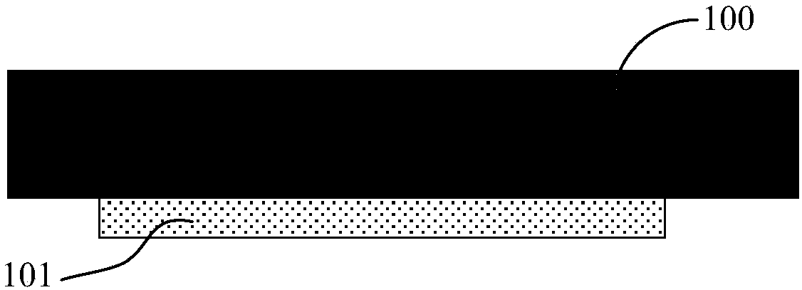
[0069] Step S1, providing a first device wafer, forming a first alignment mark on the first device wafer, wherein the shape of the first alignment mark is a ring;

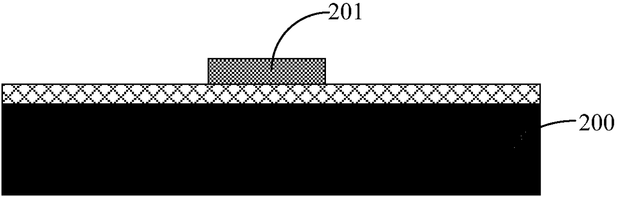
[0070] Step S2, providing a second device wafer, and forming a second alignment mark on the second device wafer;

[0071] Step S3, forming a dielectric layer to cover the surface of the second device wafer on which the second alignment mark is formed, and the surface of the dielectric layer is flush with the surface of the second alignment mark;

[0072] Step S4, forming a dummy bonding layer surrounding the second alignment mark on the dielectric layer;

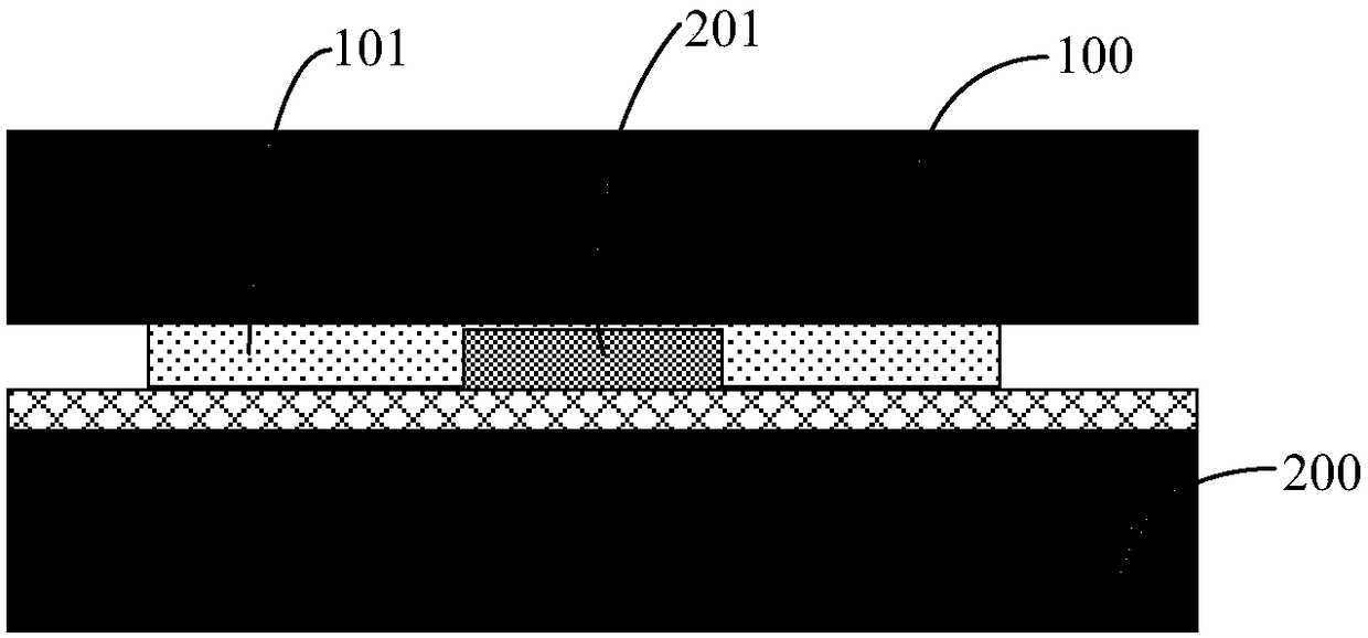
[0073] Step S5, bonding the first device wafer and the second device wafer, wherein the first alignment mark and the dummy bonding layer are aligned and bonde...

Embodiment 2

[0146] The present invention also provides a semiconductor device, which can detect the bonding alignment accuracy of the semiconductor device by using the detection method of the first embodiment.

[0147] Such as Figure 2G and Figure 2H As shown, the semiconductor device mainly includes:

[0148] A first device wafer 300, on which a first alignment mark 3021 is formed, wherein the shape of the first alignment mark 3021 is ring-shaped;

[0149] A second device wafer 400, on which a second alignment mark 4021 is formed;

[0150] A dielectric layer 403 is formed on the surface of the second device wafer 400 on which the second alignment mark 4021 is formed, and the surface of the dielectric layer 403 is flush with the surface of the second alignment mark 4021;

[0151] A dummy bonding layer surrounding the second alignment mark 4021 is formed on the dielectric layer 403;

[0152] The first device wafer 300 and the second device wafer 400 are bonded, wherein the first alig...


PUM


Abstract

The invention provides a bonding alignment precision detection method and a semiconductor device and relates to the technology field of a semiconductor. The detection method comprises steps that a first device wafer is provided, a first alignment mark is formed on the first device wafer, and the shape of the first alignment mark is annular; a second device wafer is provided, and a second alignmentmark is formed on the second device wafer; a dielectric layer is formed to cover the surface of the second device wafer on which the second alignment mark is formed, and the surface of the dielectriclayer is flush with the surface of the second alignment mark; a virtual bonding layer around the second alignment mark is formed on the dielectric layer; the first device wafer and the second devicewafer are bonded, the first alignment mark and a virtual bonding layer are aligned and bonded, and the second alignment mark is opposite to a blank area surrounded by the first alignment mark; a pattern formed by the first alignment mark and the second alignment mark is imaged to detect bonding alignment precision.

Description

technical field [0001] The invention relates to the technical field of semiconductors, in particular to a method for detecting bonding alignment accuracy and a semiconductor device. Background technique [0002] Wafer bonding technology is widely used in three-dimensional integrated circuits (3D IC), micro-electromechanical systems (MEMS), CMOS image sensors (CIS), silicon-on-insulator (SOI) and other fields. Usually, the bonding between the device wafer and the bare silicon chip does not require high alignment accuracy, while the alloy bonding between the device wafer and the device wafer usually requires device structure and electrical interconnection. High alignment accuracy. With the development of semiconductor technology, the complexity and integration of 3D devices will become higher and higher, and the requirements for bonding alignment accuracy will also increase. Infrared light sources are usually used to penetrate the wafer to identify the detection pattern of a...

Claims


Application Information

Patent Timeline
IPC IPC(8): H01L21/66H01L23/544
CPCH01L22/12H01L22/34
Inventor 程晋广陈福成施林波
Owner SEMICON MFG INT (SHANGHAI) CORP
Why Eureka
Try Eureka