
Semiconductor device and formation method thereof

A semiconductor and device technology, applied in the field of semiconductor devices and their formation, can solve problems such as complex semiconductor device processes, and achieve the effects of simplifying the process and avoiding tunneling leakage.

Active Publication Date: 2018-06-29
SEMICON MFG INT (SHANGHAI) CORP +1
View PDF8 Cites 2 Cited by
  • Summary
  • Abstract
  • Description
  • Claims
  • Application Information

AI Technical Summary

Problems solved by technology

[0004] However, whether it is a planar MOS transistor or a semiconductor device composed of a fin field effect transistor, the process is relatively complicated.

Method used


Image

  • Semiconductor device and formation method thereof
  • Semiconductor device and formation method thereof
  • Semiconductor device and formation method thereof

Examples


Embodiment Construction

[0027] As mentioned in the background, the process of forming semiconductor devices in the prior art is relatively complicated.

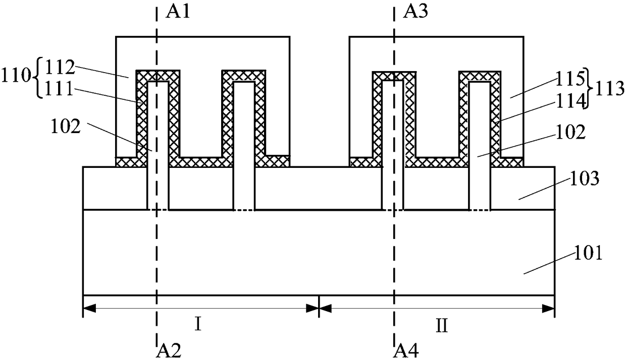
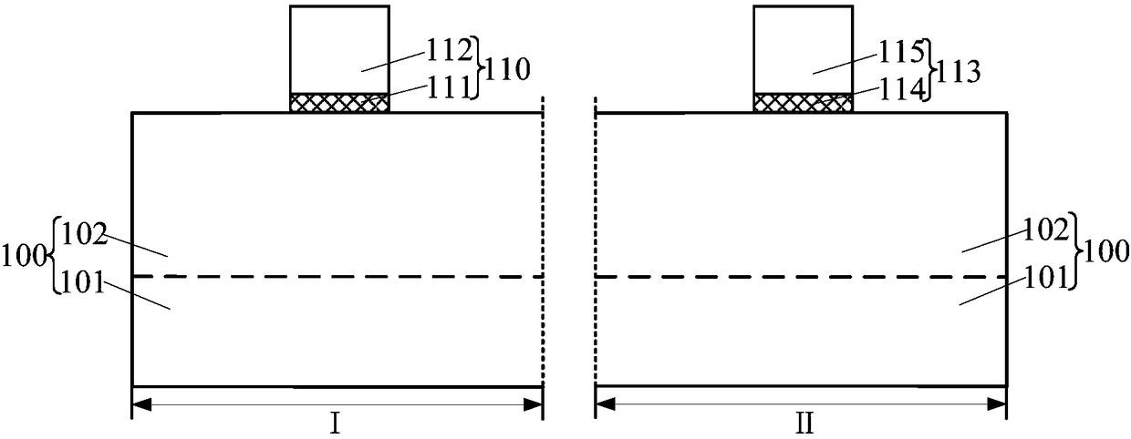
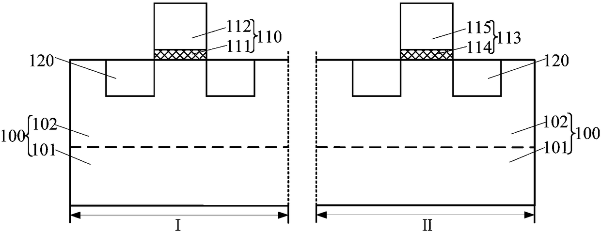
[0028] A method for forming a semiconductor device, comprising: providing a semiconductor substrate, the semiconductor substrate includes a core region and an edge region, the semiconductor substrate in the core region has a first gate structure, and the semiconductor substrate in the edge region There is a second gate structure on the bottom; a first source-drain doped layer is formed in the semiconductor substrate in the core area on both sides of the first gate structure; a second source is formed in the semiconductor substrate in the edge area on both sides of the second gate structure. Drain doped layer.

[0029] In order to avoid tunneling leakage between the source-drain doped layer in the edge region and the semiconductor substrate in the edge region, the ion concentration in the second source-drain doped layer is required to be lower than t...


PUM


Abstract

The invention relates to a semiconductor device and a formation method thereof. The method includes the following steps that: a substrate is provided, wherein the substrate comprises a core region andan edge region, wherein the substrate is provided with a first gate structure at the core region and is provided with a second gate structure at the edge region; source / drain doped layers are formedin the core edge of the substrate at two sides of the first gate structure and in the edge region of the substrate at two sides of the second gate structure respectively, and first ions are arranged in the source / drain doped layers; and the source / drain doped layers at the edge region are doped with second ions, and the conductivity type of the second ions is opposite to the conductivity type of the first ions. With the method adopted, the process of the semiconductor device can be simplified.

Description

technical field [0001] The invention relates to the field of semiconductor manufacturing, in particular to a semiconductor device and a forming method thereof. Background technique [0002] MOS transistors are one of the most important components in modern integrated circuits. The basic structure of a MOS transistor includes: a semiconductor substrate; a gate structure located on the surface of the semiconductor substrate, a source region located in the semiconductor substrate on one side of the gate structure, and a drain region located in the semiconductor substrate on the other side of the gate structure. The working principle of the MOS transistor is: by applying a voltage to the gate structure, the current through the channel at the bottom of the gate structure is adjusted to generate a switching signal. [0003] With the development of semiconductor technology, the ability of the traditional planar MOS transistor to control the channel current becomes weaker, resultin...

Claims


Application Information

Patent Timeline
Patent Type & Authority Applications(China)
IPC IPC(8): H01L21/8234H01L27/088
CPCH01L21/823431H01L27/0886H01L21/823418H01L27/088H01L29/6659H01L29/7833
Inventor 周飞
Owner SEMICON MFG INT (SHANGHAI) CORP
Features
  • Generate Ideas
  • Intellectual Property
  • Life Sciences
  • Materials
  • Tech Scout
  • Unparalleled Data Quality
  • Higher Quality Content
  • 60% Fewer Hallucinations
Learn More