Display panel and manufacturing method thereof

A technology for a display panel and a manufacturing method, which is applied to the manufacturing of semiconductor/solid-state devices, electrical components, and electrical solid-state devices, etc., can solve problems such as display defects and pixel light leakage of OLED display panels, and achieve the effect of improving display effect and eliminating pixel light leakage.

Inactive Publication Date: 2018-06-29
SHENZHEN CHINA STAR OPTOELECTRONICS SEMICON DISPLAY TECH CO LTD
View PDF10 Cites 23 Cited by
  • Summary
  • Abstract
  • Description
  • Claims
  • Application Information

AI Technical Summary

Problems solved by technology

[0003] For large-size and high-resolution OLED display panels, the top emission structure can meet the aperture ratio requirements, but no matter what kind of manufacturing process is used, there is a problem of light leakage from the pixels (that is, the OLED functional layer), so that the OLED display panel has display defects.

Method used


Image

  • Display panel and manufacturing method thereof
  • Display panel and manufacturing method thereof
  • Display panel and manufacturing method thereof

Examples


Embodiment approach

[0038] Here, the manufacturing method of the thin film transistor according to the embodiment of the present invention is constituted by steps 1 to 5, and the method of manufacturing the thin film transistor in this way is only one embodiment of the present invention, and the manufacturing method of the thin film transistor of the present invention is not limited here.

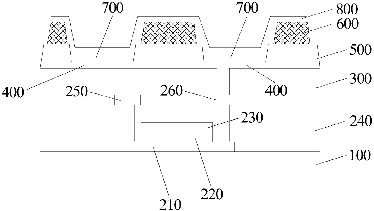
[0039] Step 6: Reference Figure 2F A planarization layer 300 is formed on the second insulating layer 240 , the source electrode 250 and the drain electrode 260 .

[0040] Step Seven: Refer to Figure 2G , fabricating and forming an anode 400 penetrating through the planar layer 300 to be connected to the drain 260 on the planar layer 300 . In this embodiment, the anode 400 has high reflectivity.

[0041] Step Eight: Reference Figure 2H 1. On the anode 400 and the planarization layer 300, a stacked pixel definition layer 500 and a light shielding layer 600 are formed.

[0042]Step Nine: Reference Figu...


PUM


Abstract

The invention provides a display panel which comprises a substrate, a flat body, an anode, a pixel defining layer, a shading layer, an OLED (Organic Light Emitting Diode) functional layer and a cathode, wherein a thin film transistor is arranged on the substrate; the flat layer is arranged on the thin film transistor; the anode is arranged on the flat layer and penetrates through the flat layer tobe connected with the thin film transistor; the pixel defining layer is arranged on the flat layer; the shading layer is arranged on the pixel defining layer; pixel defining holes for exposing the anode are formed in the shading layer and the pixel defining layer; the OLED functional layer is arranged on the exposed anode; and the cathode is arranged on the shading layer and the OLED functional layer. The invention further provides a manufacturing method of the display panel. The shading layer is formed on the pixel defining layer, so that light leaking from the side of the OLED functional layer in the pixel defining hole can be shaded; and therefore, the pixel light leakage problem in the prior art can be eliminated, and the display effect of the display panel is further improved.

Description

technical field [0001] The invention belongs to the field of display technology, and in particular relates to a display panel and a manufacturing method thereof. Background technique [0002] In recent years, organic light-emitting diode (Organic Light-Emitting Diode, OLED) display panel has become a very popular emerging flat display panel product at home and abroad, because OLED display panel has self-illumination, wide viewing angle, short response time, high luminous efficiency, It has the characteristics of wide color gamut, thin thickness, large-size and flexible display panel and simple manufacturing process, and it also has the potential of low cost. [0003] For large-size and high-resolution OLED display panels, the top emission structure can meet the aperture ratio requirements, but no matter what kind of manufacturing process is used, there is a problem of light leakage from pixels (that is, OLED functional layers), so that OLED display panels have display defect...

Claims


Application Information

Patent Timeline
Patent Type & Authority Applications(China)
IPC IPC(8): H01L27/32H01L51/52H01L21/77
CPCH10K59/12H10K50/86H10K59/1201H10K59/122H10K50/865
Inventor 张良芬任章淳
Owner SHENZHEN CHINA STAR OPTOELECTRONICS SEMICON DISPLAY TECH CO LTD
Why Eureka
Try Eureka