
Patsnap Eureka
For R&D, Patsnap Eureka makes reading and utilizing patents & technical documents easy.
Patsnap Eureka AIR
Designed for self-driven R&D workflows. Generate viable solutions, solve complex R&D challenges, empower your innovation with AI.

Patsnap Eureka Materials
Designed for material experts only. Revolutionize your material R&D, from search, analyze, to developing new materials.

TechResearch
Generate reliable direction feasibility study reports for your R&D in just a few steps.

TechSeek
Discover and master advanced knowledge NOW. Basics, ideas, possibilities, all at once.

TechMind
As an expert in R&D Theories, TechMind can generates customized viable solutions instantly.

TechRisk
Analyze your overall solution with one click, know your potential R&D risks in advance.

TechMonitor
Get weekly tech updates, stay abreast of the latest tech innovations and key insights.
Semiconductor device and manufacturing method thereof
A manufacturing method, semiconductor technology, applied in semiconductor/solid-state device manufacturing, semiconductor devices, semiconductor/solid-state device components, etc., to avoid sticking and product failure problems, and avoid electrostatic effects
- Summary
- Abstract
- Description
- Claims
- Application Information
AI Technical Summary
Problems solved by technology
Method used
Image

Examples
Embodiment 1
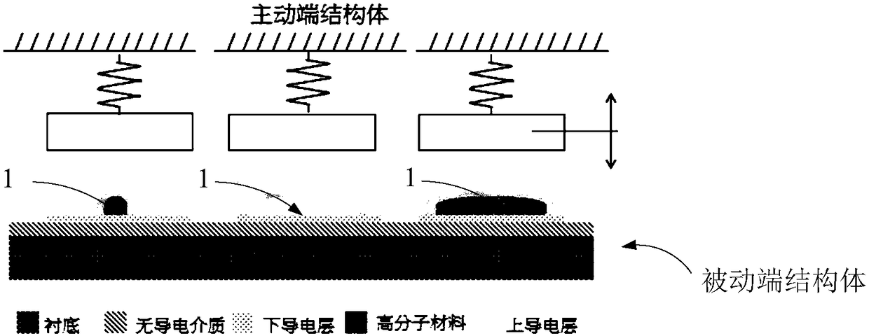
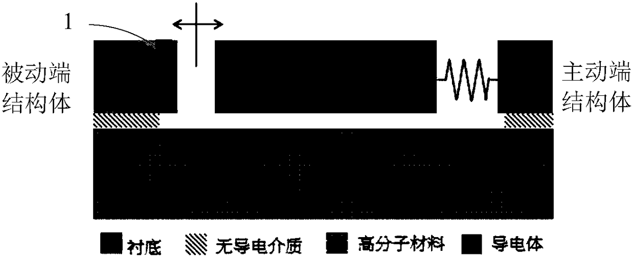
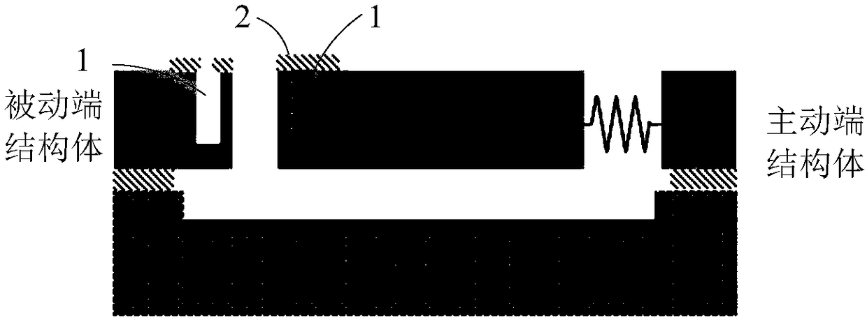
[0063] Embodiment 1 of the present application provides a semiconductor device, figure 1 is a schematic diagram of the semiconductor device of this embodiment.
[0064] Such as figure 1 As shown, the semiconductor device may have an active end structure and a passive end structure, and the active end structure and the passive end structure can move relative to each other and contact each other.
[0065] In this example, if figure 1 As shown, at least one of the active end structure and the passive end structure has a cavity 1, and the cavity is formed as an accommodating space. The cavity can be surrounded by a bottom and an outer wall, and both the outer wall and the bottom are conductive. material, wherein the outer wall is the upper conductive layer in the figure, and the bottom is the lower conductive layer in the figure. Wherein, the outer wall protrudes in the direction of relative movement relative to the bottom, and the part where the active end structure and the pa...
PUM
 Abstract
Description
Claims
Application Information
 - R&D Engineer
- R&D Manager
- IP Professional
- Industry Leading Data Capabilities
- Powerful AI technology
- Patent DNA Extraction
Browse by: Latest US Patents, China's latest patents, Technical Efficacy Thesaurus, Application Domain, Technology Topic, Popular Technical Reports.
© 2024 PatSnap. All rights reserved.Legal|Privacy policy|Modern Slavery Act Transparency Statement|Sitemap|About US| Contact US: help@patsnap.com