

Digital logic operation method and circuit and FPGA chip
A technology of digital logic and arithmetic circuits, applied in electrical digital data processing, digital data processing components, calculations, etc., can solve the problems of large delay, long cycle, low system operation rate, etc., to reduce delay and operation. Period, the effect of reducing the maximum delay
- Summary
- Abstract
- Description
- Claims
- Application Information
AI Technical Summary
Problems solved by technology
Method used
Image

Examples
no. 1 example
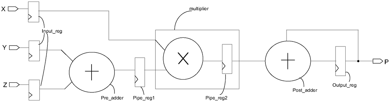
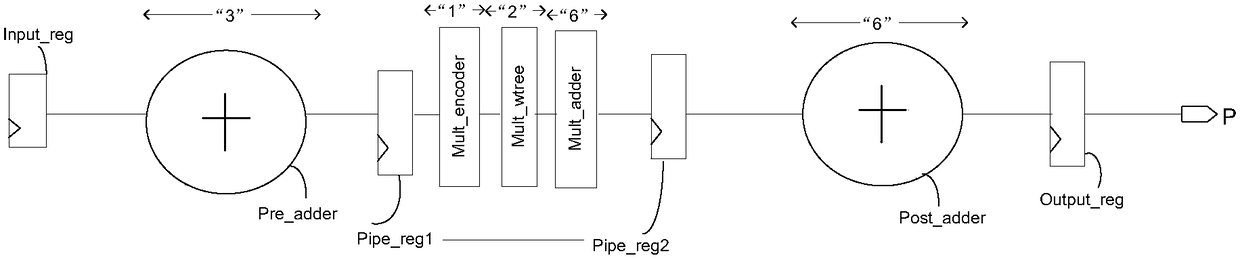
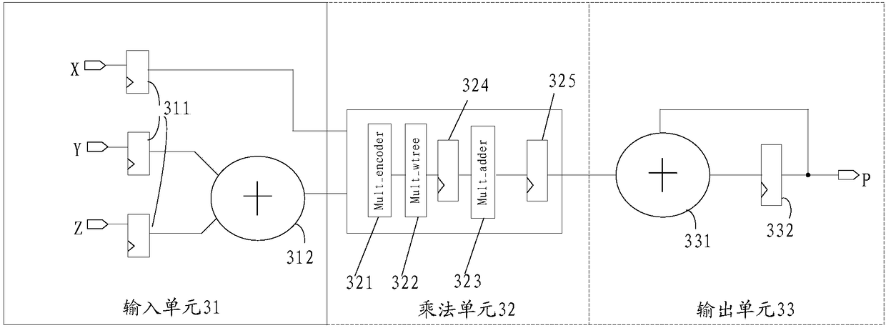
[0030] Please refer to image 3 , image 3 It is a schematic circuit structure diagram of a digital logic operation circuit provided by the first embodiment of the present invention, including an input unit 31, a multiplication unit 32 and an output unit 33 connected in sequence;
[0031] The input unit 31 includes several input registers 311 for receiving input data respectively;
[0032] The multiplication unit 32 comprises an encoder 321, a Wallace tree structure module 322 and an adder 323 connected in sequence, the first pipeline register 324 is arranged between any two devices in the multiplication unit 32, and the second pipeline register 325 is arranged in the adder after 323;
[0033] The output unit 33 includes an accumulator 331 and an output register 332 connected in sequence, and the output of the accumulator 331 and the output of the multiplication unit 32 serve as the input of the accumulator 331 .
[0034] The digital logic operation circuit in the present e...
no. 2 example
[0045] Please refer to Figure 5 , Figure 5 A flow chart of a digital logic operation method provided in the second embodiment of the present invention, including:
[0046] S501. The input register in the output unit receives input data;
[0047] S502. The input data is input to the multiplication unit, and the multiplication operation is performed through the encoder, the Wallace tree structure module and the adder in the multiplication unit in turn to obtain the operation data; wherein, a second device is set between any two devices in the multiplication unit. A water register is provided with a second water register after the adder;
[0048] S503. An operation data input and output unit, the output unit includes an accumulator and an output register connected in sequence, and the output of the accumulator and the output of the multiplication unit are used as the input of the accumulator.
[0049] The digital logic operation circuit in this embodiment roughly includes th...
PUM
 Abstract
Description
Claims
Application Information