LED die bonder and die bonding method

A technology of LED die bonding machine and die bonding machine, which is applied in the manufacture of semiconductor/solid-state devices, electrical components, circuits, etc., can solve the problems of poor accuracy and reduced die bonding speed, so as to improve production efficiency and save loading and unloading time. Effect

Active Publication Date: 2018-07-06
深圳市微恒自动化设备有限公司
View PDF5 Cites 0 Cited by
  • Summary
  • Abstract
  • Description
  • Claims
  • Application Information

AI Technical Summary

Problems solved by technology

[0005] The technical problem to be solved by the present invention is to provide an LED crystal bonder and a crystal bond method, aiming to solve the problems of the LED crystal bonder in the prior art, such as the reduction of the crystal bond speed and the accuracy Variation problem

Method used


Image

  • LED die bonder and die bonding method
  • LED die bonder and die bonding method
  • LED die bonder and die bonding method

Examples


Embodiment Construction

[0034] In order to make the technical problems, technical solutions and beneficial effects to be solved by the present invention clearer, the present invention will be further described in detail below in conjunction with the accompanying drawings and embodiments. It should be understood that the specific embodiments described here are only used to explain the present invention, not to limit the present invention.

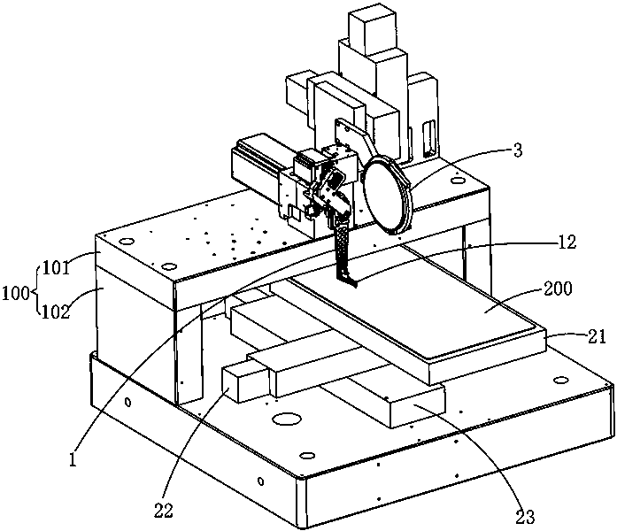
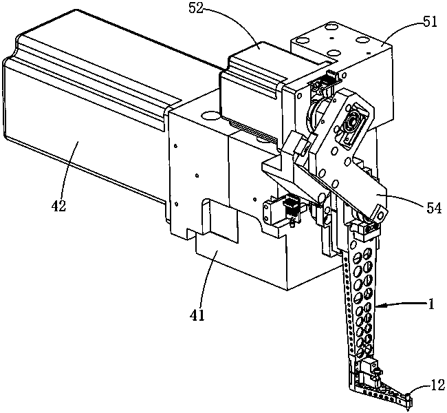
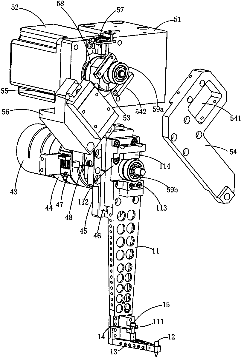
[0035] The invention provides an LED crystal bonding machine, which includes a workbench system for moving the LED frame, a wafer positioning system for providing wafer positioning, and a crystal bonding system for picking up the chip and fixing the chip on the LED frame, the crystal bonding system Including a solid crystal arm and a driving mechanism for picking up and moving the wafer, the workbench system has a workbench for placing the LED frame, the wafer positioning system includes a crystal ring, and the wafer is placed on the crystal ring;

[0036] The wafe...


PUM


Abstract

The invention is suitable for the technical field of LED packaging equipment, and provides an LED die bonder and a die bonding method. The LED die bonder comprises a workbench system which is used formoving an LED frame, a die positioning system which is used for providing die positioning and a die bonding system which picks up the die and fixes the die on the LED frame. The stroke size change ofthe workbench system and movement of the die positioning system have no mutual influence so as to have no collision; and the die bounder can be adaptive to different sizes of LED frames by only controlling the stroke of the workbench system without extending the die bonding arm so that the die bonding accuracy and speed of the large-size LED frame can be effectively enhanced. The super-large andsuper-wide LED frame can be manufactured, and the conventional small LED frames can be spliced so that the material loading and unloading time can be saved and the production efficiency can be enhanced.

Description

technical field [0001] The invention belongs to the technical field of LED packaging equipment, and in particular relates to an LED crystal bonding machine and a crystal bonding method. Background technique [0002] With the development of semiconductor technology, especially the development of LED lamp COB technology, the LED frame is getting bigger and bigger, such as ceiling lamps, the general size reaches 310mm*310mm, or even larger, and it is required to directly bond the crystal on the board (that is, stick the chip ). [0003] The workbench system of the LED die bonder on the existing market is placed horizontally with the wafer on the same level or a level with a small height difference. The movement range of the workbench system is limited, and the expansion of the movement range will collide with the wafer. The die-bonding arm swings within 90 degrees or 180 degrees in the horizontal plane to realize the die-bonding. The effective range of the die-bonding arm is l...

Claims


Application Information

Patent Timeline
Patent Type & Authority Applications(China)
IPC IPC(8): H01L33/52H01L21/67
CPCH01L33/52H01L21/67121H01L21/67126
Inventor 唐文轩
Owner 深圳市微恒自动化设备有限公司
Why Eureka
Try Eureka