n-type III-nitride semiconductor material and preparation method thereof

A nitride semiconductor, n-type technology, applied in semiconductor/solid-state device manufacturing, electrical components, circuits, etc., can solve the problems of surface morphology deterioration, hindering the growth of III-nitride materials, and reducing carrier concentration. Achieve the effect of avoiding surface deterioration, avoiding sample surface passivation and holes

Inactive Publication Date: 2018-07-10
SUZHOU NANOWIN SCI & TECH
View PDF2 Cites 0 Cited by
  • Summary
  • Abstract
  • Description
  • Claims
  • Application Information

AI Technical Summary

Problems solved by technology

For example, a layer of SiN will be formed on the surface of the sample doped with Si, and the surface will be passivated, which will hinder the growth of the subsequent III-nitride material and cause the deterioration of the surface morphology; the surface of the sample doped with Ge will form A large number of pores, which eventually lead to the deterioration of the sample surface
[0005] The main reason for the above phenomenon is that the atomic concentration of doping elements in the gas phase is too high. The above-mentioned doping impurity atoms are easy to gather on the surface, and chemically react with NH3 to form a passivation layer or migrate to each other to form balls, thereby hindering the subsequent materials. growth progress
[0006] The fundamental way to solve this problem is to reduce the impurity concentration in the gas phase, and reducing the impurity concentration in the gas phase will lead to a decrease in the carrier concentration in the sample and affect the electrical properties

Method used


Image

  • n-type III-nitride semiconductor material and preparation method thereof

Examples


preparation example Construction

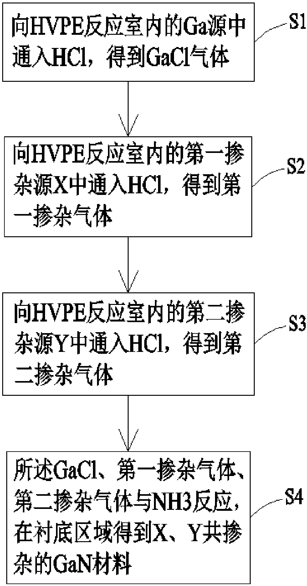
[0034] For the n-type III nitride semiconductor material doped with two dopants, the present invention provides a preparation method. The preparation method includes the following steps:

[0035] S1. Pass the reaction gas into the reaction chamber to react with the reaction source;

[0036] S2. Pass reaction gas into the first doping source X in the reaction chamber to obtain the first doping gas;

[0037] S3. Pass the reaction gas into the second doping source Y in the reaction chamber to obtain the second doping gas;

[0038] S4, the first doping gas, the second doping gas, and the product of the reaction gas and the reaction source and NH 3 After the reaction, an n-type group III nitride semiconductor material co-doped with X and Y is obtained in the substrate region.

[0039] Hereinafter, taking GaN as an example, the preparation method of the n-type III nitride semiconductor material is described in detail, which includes the following steps:

[0040] S1. Pour HCl into the Ga source...

Embodiment approach

[0046] As an embodiment, the first doping source X and the second doping source Y are selected from: Si, Ge, Sn, O, and S. Preferably, the first doping source X is Si, and the second doping source Y is Ge. At this time, the HVPE-based GaN material preparation method of the present invention adopts a multi-donor co-doping method to prepare the GaN material. In the process of HVPE growth of GaN, source gas containing Si impurities and Ge impurities are simultaneously introduced to generate n-type GaN co-doped with Si and Ge. Therefore, the concentration of the Si impurity source gas and Ge impurity source gas in the gas phase is lower than the lower limit of Si doping passivation and Ge doping holes, respectively, so that the sample morphology is not deteriorated, and the two are generated inside the GaN material The sum of the carrier concentration can meet the requirements of the device for the carrier concentration of the substrate.

[0047] Further, when the first doping sour...


PUM

PropertyMeasurementUnit
Thicknessaaaaaaaaaa

Abstract

The invention provides n-type III-nitride semiconductor material and a preparation method thereof. A first doping source X and a second doping source Y are doped in the n-type III-nitride semiconductor material. The first doping source X and the second doping source Y are selected from the elements in the family IV and the family VI. The n-type III-nitride semiconductor material includes multipledoping elements doped by multiple donors so that the problems of sample surface passivation and holes caused by excessively high concentration of the single donor impurity source gas can be avoided, the carriers in the n-type III-nitride semiconductor material are provided by the sum of the carriers generated by doping of multiple impurity sources together to realize the influence of the device onthe electrical performance of the n-type III-nitride semiconductor material substrate and thus the high-quality n-type III-nitride semiconductor material self-supporting substrate is prepared.

Description

Technical field [0001] The present invention relates to the field of semiconductor technology, in particular to an n-type III nitride semiconductor material and a preparation method thereof. Background technique [0002] Group III nitride materials (including GaN, AlN, InN and their alloy materials), commonly used growth methods include MOCVD, MBE, and HVPE growth methods. Among them, MOCVD and MBE methods have lower growth rates, and are usually used to grow GaN materials with a thickness of no more than 15 microns for the preparation of optoelectronics and microelectronic devices. The HVPE method is generally used to grow thick layer III nitride materials with a thickness greater than 15 microns. [0003] In order to realize the n-type doping of materials, the commonly used doping elements generally come from group IV elements and group VI elements. Typical doping elements include Si, Ge, Sn, O, S, etc. Due to the low growth rate of MOCVD and MBE, the high efficiency of impurit...

Claims


Application Information

Patent Timeline
IPC IPC(8): H01L21/02
CPCH01L21/0254H01L21/0257
Inventor 张育民王建峰徐科任国强徐俞蔡德敏胡晓剑
Owner SUZHOU NANOWIN SCI & TECH
Why Eureka
Try Eureka