Organic light emitting display panel and manufacturing method thereof and display device

A light-emitting display, organic technology, used in semiconductor/solid-state device manufacturing, electrical components, electrical solid-state devices, etc., can solve problems such as poor film uniformity of the light-emitting layer, and achieve the effect of improving display quality

Active Publication Date: 2018-07-13
BOE TECH GRP CO LTD
View PDF5 Cites 13 Cited by
  • Summary
  • Abstract
  • Description
  • Claims
  • Application Information

AI Technical Summary

Problems solved by technology

[0005] The inventors found that organic light-emitting display panels produced by ink-jet printing generally have the problem of poor film-forming uniformity of the light-emitting layer

Method used


Image

  • Organic light emitting display panel and manufacturing method thereof and display device
  • Organic light emitting display panel and manufacturing method thereof and display device
  • Organic light emitting display panel and manufacturing method thereof and display device

Examples


Embodiment Construction

[0026] Embodiments of the present invention are described in detail below, examples of which are shown in the drawings, wherein the same or similar reference numerals designate the same or similar elements or elements having the same or similar functions throughout. The embodiments described below by referring to the figures are exemplary only for explaining the present invention and should not be construed as limiting the present invention.

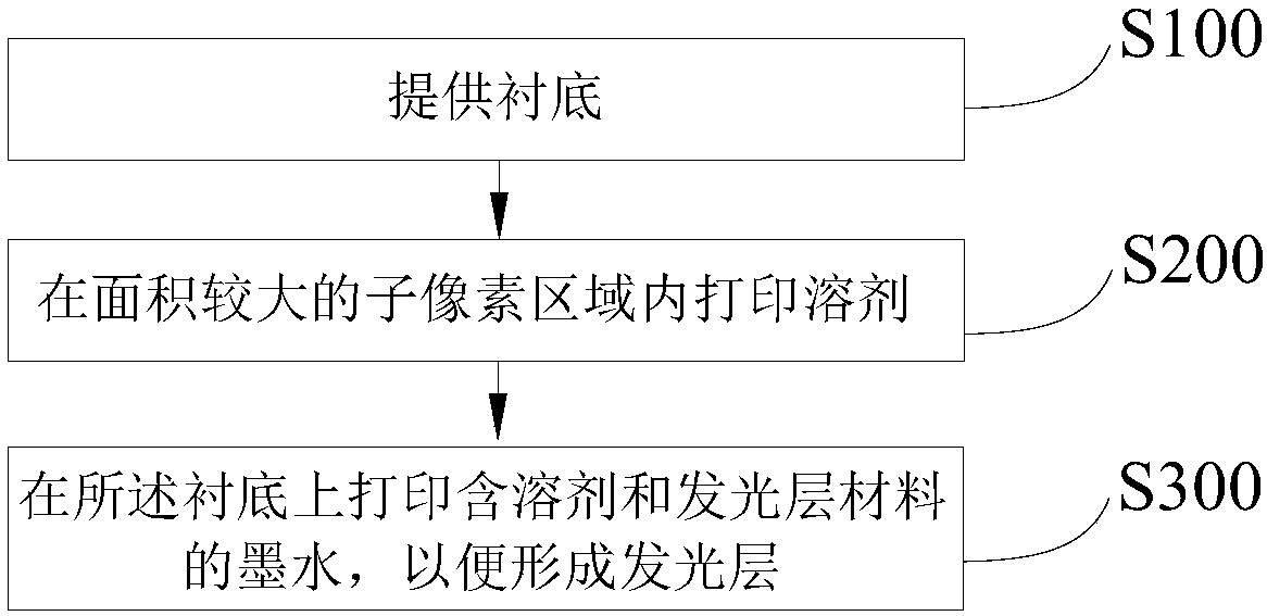
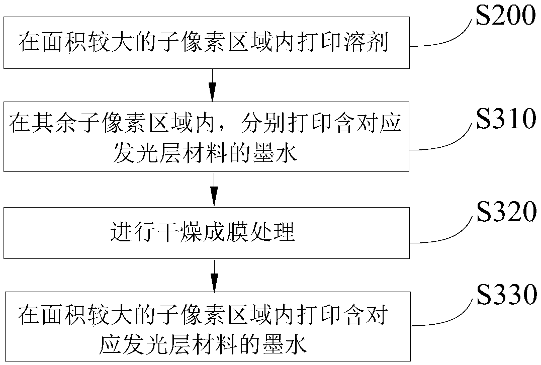
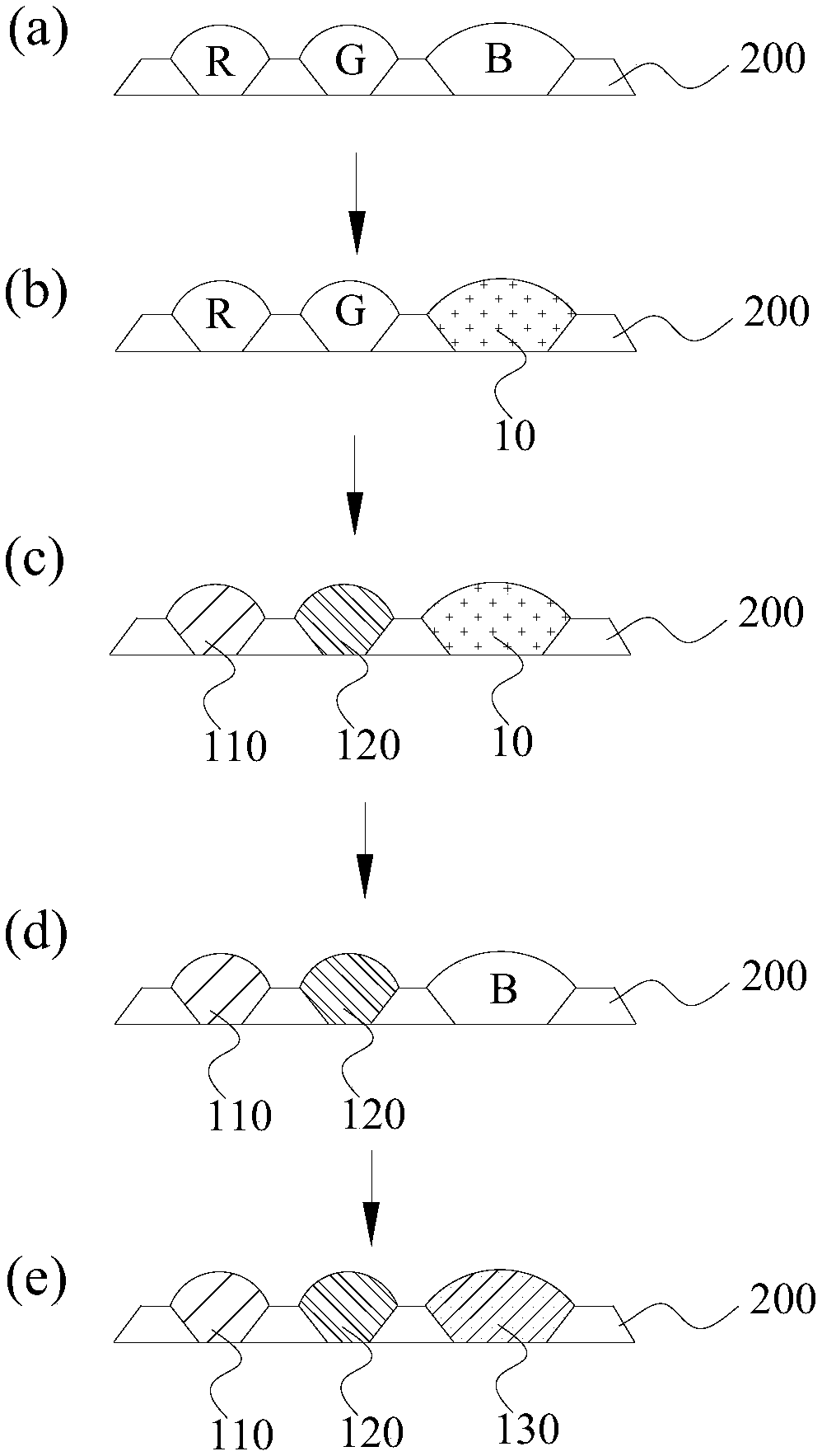
[0027] In one aspect of the invention, the invention provides a method for manufacturing an organic light emitting display panel. In this method, before printing the light-emitting layer material, the solvent of the ink containing the light-emitting layer material is printed in the sub-pixel area with a large area in advance, and the solvent can provide solvent volatilization for the ink in the sub-pixel area with a small area printed subsequently. atmosphere, thereby slowing down the volatilization speed of the ink in the sub-pixel area...


PUM


Abstract

The invention discloses an organic light emitting display panel and a manufacturing method thereof, and a display device, and particularly provides a method for manufacturing the organic light emitting display panel. The method includes the steps of providing a substrate having a pixel defining layer which defines multiple sub pixel areas different in area and then printing with ink containing solvent and luminous layer materials on the substrate to form a luminous layer on the basis of the pixel defining layer, wherein the solvent is printed in large-area sub pixel area in advance before inkprinting. Ink volatilizing speed in ink printing in other small-area sub pixel areas can be reduced, film forming uniformity of the small-area sub pixel areas is improved, and further OLED display quality is improved.

Description

technical field [0001] The present invention relates to the field of display technology, in particular, to an organic light emitting display panel, a manufacturing method thereof, and a display device. Background technique [0002] Organic electroluminescence (OLED) display technology is characterized by self-illumination, wide viewing angle, high contrast ratio, low power consumption, extremely high response speed, ultra-thin weight, flexible display, rollable screen, strong temperature adaptability, and simple manufacturing process, etc. Advantages, has become a research hotspot in the field of optoelectronic display technology. As an important kind of OLED display technology, polymer electroluminescence (PLED) display technology is more and more widely used. The technology of preparing PLED display devices by inkjet printing (inkjet printing PLED technology) is widely used in the production of organic light-emitting display panels due to its advantages of simple operatio...

Claims


Application Information

Patent Timeline
Patent Type & Authority Applications(China)
IPC IPC(8): H01L27/32H01L51/56
CPCH10K59/352H10K71/135H10K71/15H10K59/1201H10K71/00
Inventor 崔颖侯文军
Owner BOE TECH GRP CO LTD
Why Eureka
Try Eureka