Semiconductor structure and manufacturing method thereof

A manufacturing method and semiconductor technology, applied in the fields of semiconductor/solid-state device manufacturing, semiconductor devices, semiconductor/solid-state device components, etc., can solve problems such as increased complexity, signal interference, and complex semiconductor components

Inactive Publication Date: 2018-07-27
NAN YA TECH
View PDF4 Cites 1 Cited by
  • Summary
  • Abstract
  • Description
  • Claims
  • Application Information

AI Technical Summary

Problems solved by technology

[0003] However, the manufacturing and integration of semiconductor devices involves many complicated steps and operations
Integrating semiconductor devices with small profile and high density is becoming more and more complex
The increased complexity of manufacturing and integrating semiconductor components can lead to defects such as poor electrical interconnection, signal interference, component delamination, or high yield loss

Method used


Image

  • Semiconductor structure and manufacturing method thereof
  • Semiconductor structure and manufacturing method thereof
  • Semiconductor structure and manufacturing method thereof

Examples


Embodiment Construction

[0060] The following description of the disclosure, accompanied by the accompanying drawings, which are incorporated in and constitute a part of the specification, illustrate embodiments of the disclosure to which, however, the disclosure is not limited. In addition, the following embodiments can be properly integrated to complete another embodiment.

[0061]"An embodiment," "an embodiment," "an exemplary embodiment," "another embodiment," "another embodiment" and the like mean that the embodiments described in the present disclosure may include a particular feature, structure, or characteristic, but Not every embodiment must include the particular feature, structure or characteristic. Also, repeated use of the phrase "in an embodiment" does not necessarily refer to the same embodiment, but could be the same embodiment.

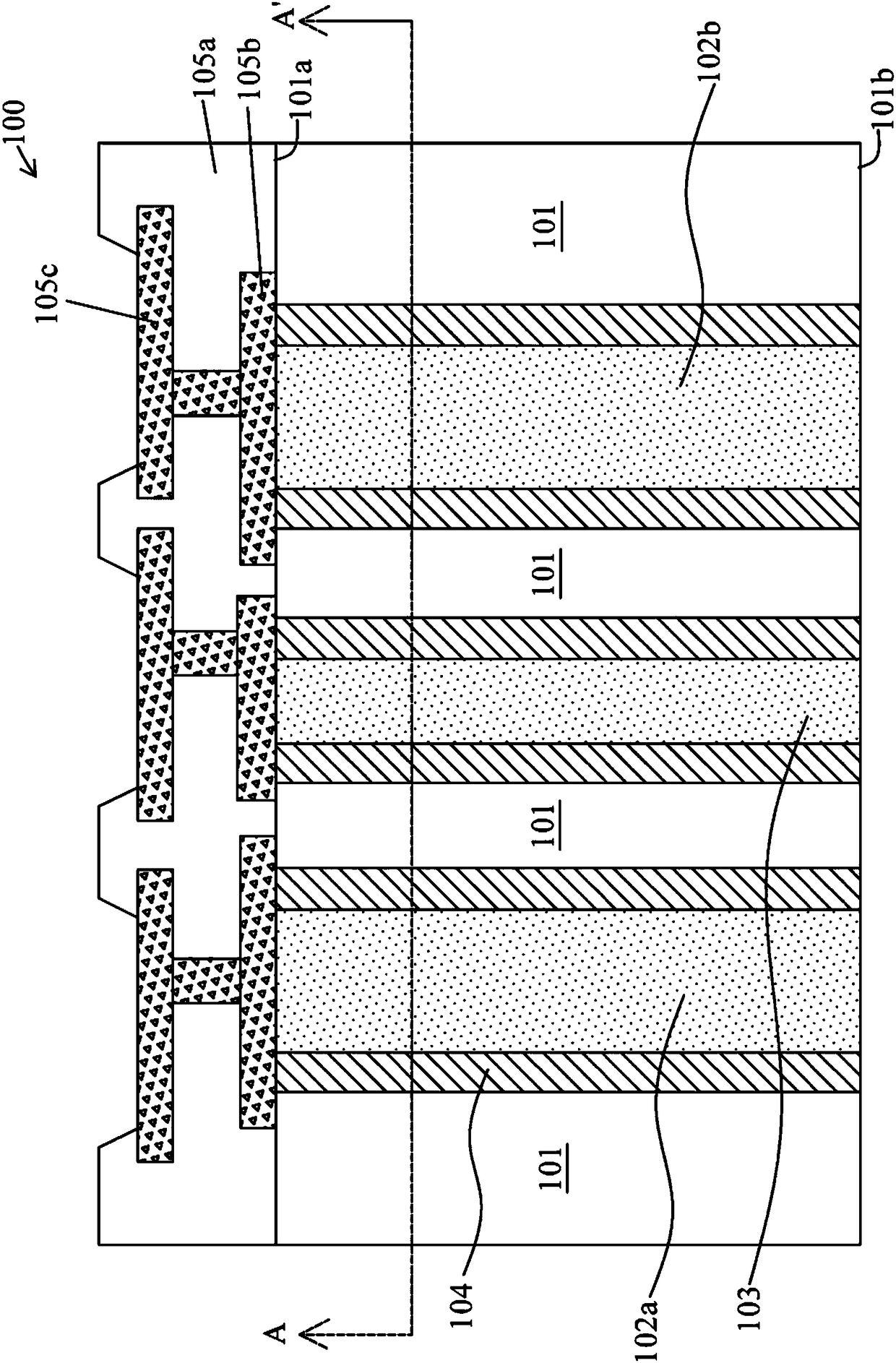
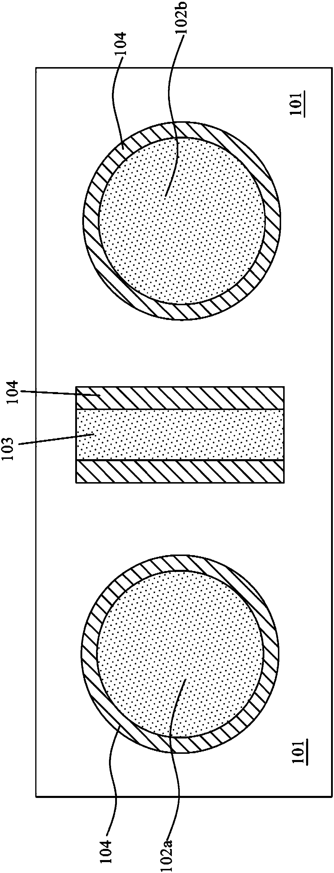
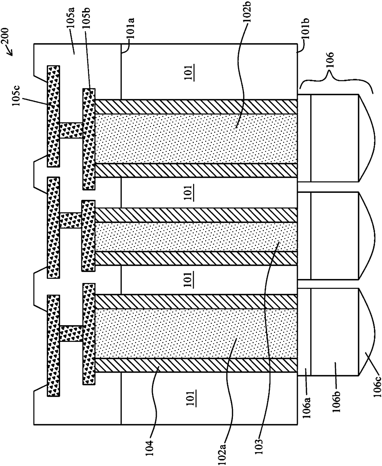
[0062] The present disclosure relates to a semiconductor structure having a metal structure between two adjacent plugs. The plug is electrically connected ...


PUM


Abstract

A semiconductor structure includes a substrate including a first side and a second side opposite to the first side; a first via extending through the substrate; a second via extending through the substrate; and a metallic structure disposed between the first via and the second via, wherein the first via is isolated from the second via by the metallic structure, the first via and the second via areconfigured to connect to a signal source or transmit a signal, and the metallic structure is configured to connect to a power or a ground.

Description

technical field [0001] The present disclosure relates to a semiconductor structure, and more particularly to a shielding structure in the semiconductor structure. Furthermore, the present disclosure relates to a method of manufacturing a semiconductor structure having the shielding structure. Background technique [0002] Semiconductor components are important to many modern applications. With the development of electronic technology, the size of semiconductor components is getting smaller and smaller, while the functions are getting bigger and the amount of integrated circuits is getting more and more. Due to the miniaturization of semiconductor devices, semiconductor devices of various forms and sizes with different functions are integrated and packaged in a single module. Furthermore, many fabrication steps are performed to integrate various forms of semiconductor elements. [0003] However, the fabrication and integration of semiconductor devices involves many complic...

Claims


Application Information

Patent Timeline
Patent Type & Authority Applications(China)
IPC IPC(8): H01L23/552H01L21/768
CPCH01L21/76838H01L23/552H01L24/05H01L24/06H01L24/13H01L24/94H01L2224/0401H01L2224/05567H01L2224/0557H01L2224/06181H01L2224/13082H01L2224/16145H01L2224/16227H01L2224/94H01L2924/10252H01L2924/10253H01L2924/10329H01L2924/15787H01L2924/15788H01L2924/3025H01L21/76898H01L23/481H01L2224/03H01L2224/11H01L23/585H01L24/14
Inventor 林柏均
Owner NAN YA TECH
Why Eureka
Try Eureka