Substrate and manufacturing method of substrate

A manufacturing method and substrate technology, which are applied in the direction of multi-layer circuit manufacturing, electrical connection of printed components, printed circuit components, etc. Effect

Inactive Publication Date: 2020-10-09
MEIKO ELECTRONICS CO LTD
View PDF8 Cites 0 Cited by
  • Summary
  • Abstract
  • Description
  • Claims
  • Application Information

AI Technical Summary

Problems solved by technology

In particular, semiconductors using Si will cause malfunctions and failures when the ambient temperature becomes 100°C or higher.

Method used


Image

  • Substrate and manufacturing method of substrate
  • Substrate and manufacturing method of substrate
  • Substrate and manufacturing method of substrate

Examples


Embodiment Construction

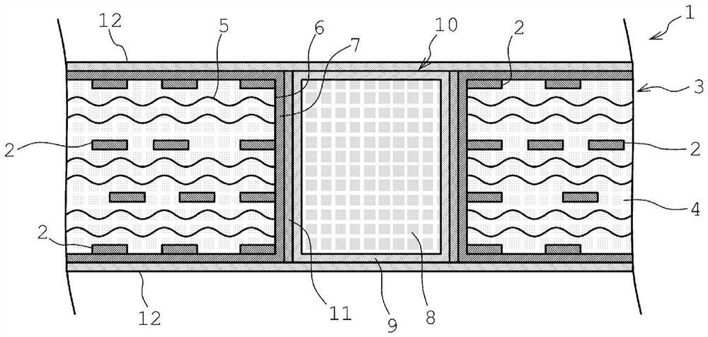
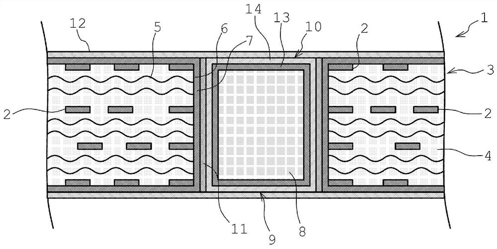
[0034] Such as figure 1 As shown, the substrate 1 of the present invention is mainly constituted by a laminated wiring board 3 called a multilayer board (including double-sided boards) on which a plurality of conductive layers 2 are formed. exist figure 1 In the example of , a so-called four-layer board formed with four conductive layers 2 is shown. The conductive layer 2 is formed on each layer as a conductive pattern. An insulating layer 4 is disposed between the conductive layers 2 . The insulating layer 4 is formed of insulating materials such as prepreg, for example.

[0035] Through holes 6 are formed in the laminated wiring board 3 . The through hole 6 penetrates the laminated wiring board 3 . The hole shape of the through hole 6 is substantially cylindrical. In plan view of laminated wiring board 3 viewed from above, through hole 6 draws a circular shape. A through hole plating layer 7 is formed on the inner wall of the through hole 6 . This through-hole platin...


PUM


Abstract

A substrate (1) is provided with: a laminated wiring board (3) on which a plurality of conductive layers (2) are formed; a through hole (6) formed by penetrating the laminated wiring board (3); a through hole plating (7), which covers the inner wall of the through hole (6), and is electrically connected to the conductive layers (2); a metal piece (10), which is disposed on the inner side of the through hole plating (7), and is configured from a core section (8), and a film section (9) covering the whole surface of the core section (8); and an alloy film (11), which is disposed between the film section (9) and the through hole plating (7), and is formed of metals which the film section (9) and the through hole plating (7) are respectively formed of.

Description

technical field [0001] The present invention relates to a substrate and a method for manufacturing the substrate. The substrate is a substrate such as a printed wiring board, in which a metal sheet is embedded, and has excellent large current characteristics and heat dissipation characteristics. Background technique [0002] Semiconductor elements in circuits tend to generate more heat due to higher densities and higher currents. In particular, semiconductors using Si cause malfunctions and failures when the ambient temperature becomes 100° C. or higher. Examples of such heat generating components such as semiconductor elements include switching elements such as IGBT (Insulated Gate Bipolar Transistor) and IPM (Intelligent Power Module). [0003] In order to effectively cool the heat-generating component, the heat-dissipating path is formed so that the heat generated from the heat-generating component dissipates toward the opposite side of the substrate. Specifically, cool...

Claims


Application Information

Patent Timeline
Patent Type & Authority Patents(China)
IPC IPC(8): H05K1/11H05K3/40H05K3/46
CPCH05K1/11H05K3/40H05K3/46
Inventor 关保明高林纯平牧野直之
Owner MEIKO ELECTRONICS CO LTD
Why Eureka
Try Eureka