Lead-free electroplating method based on reserved larger finger connection position
A connection position, leadless technology, applied in the direction of transfer printing, electrical components, printed circuits, etc., can solve the problem of corroded signal lines, etc., to achieve the effect of preventing corrosion of the gold surface, improving corrosion resistance, and improving appearance
- Summary
- Abstract
- Description
- Claims
- Application Information
AI Technical Summary
Problems solved by technology
Method used
Image
Examples
Embodiment 1
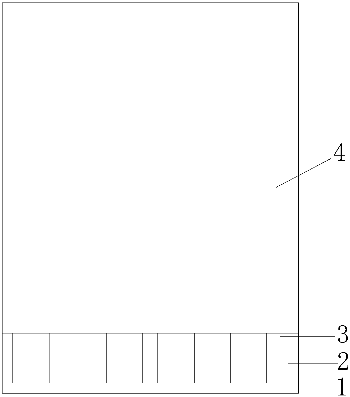
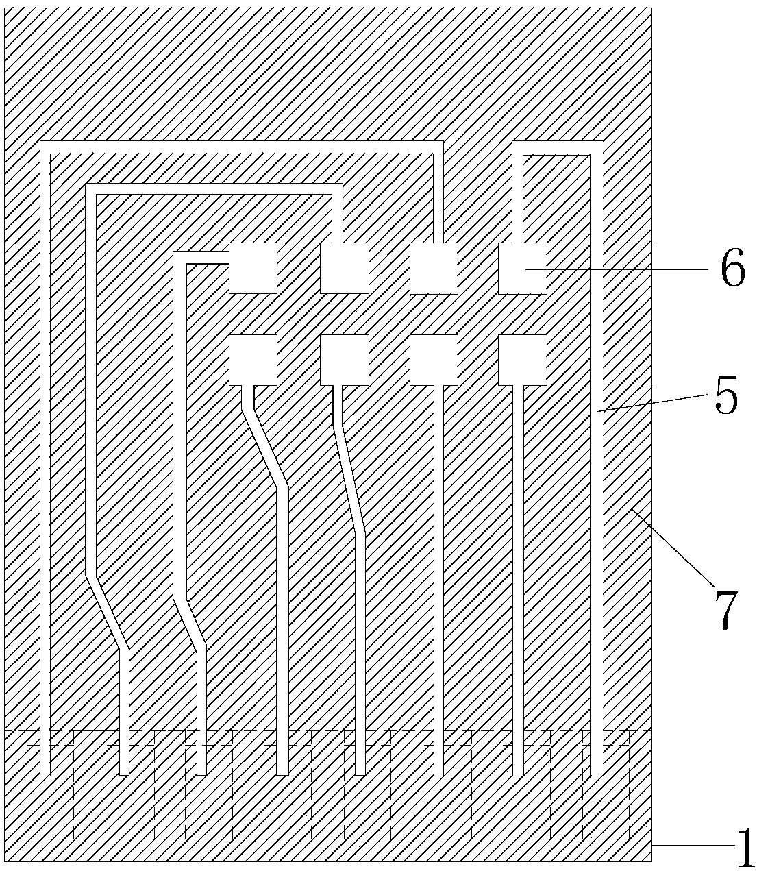
[0028] Such as figure 1 and figure 2 As shown in this embodiment, a leadless electroplating method based on pre-large finger connection positions includes the following processing steps in sequence:
[0029] (1) Cutting: cut out the core board according to the panel size of 320mm×420mm, the thickness of the core board is 0.5mm, and the thickness of the outer copper surface of the core board is 0.5OZ.
[0030] (2), making the inner layer circuit (negative film process): according to the pattern positioning hole, use a vertical coating machine to coat the photosensitive film on the core plate. Grid exposure ruler (21 grid exposure ruler) completes the exposure of the inner layer circuit, after development, the inner layer circuit pattern is formed on the core board; inner layer etching, the core board after exposure and development is etched out of the inner layer circuit, the inner layer line width The measurement is 3mil; AOI on the inner layer, and then check the open and ...
Embodiment 2
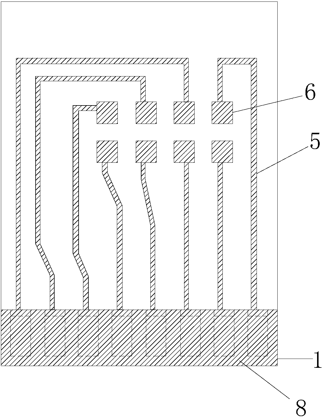
[0047] A leadless electroplating method based on the pre-enlargement of the finger connection shown in this embodiment is basically the same as that of Embodiment 1, except that in step (11), when making the outer layer circuit, it is made by a negative film process, details as follows:
[0048] (11), making the outer layer circuit (negative film process): on the production board, use a vertical coating machine to coat photosensitive film 8, the film thickness of photosensitive film is controlled 8 μ m, adopt a fully automatic exposure machine, with 5-6 grid exposure ruler ( 21 grid exposure ruler) to complete the exposure of the outer layer circuit, after development, the outer layer circuit pattern 5 is formed in the outer layer circuit area of the production board, and the outer layer circuit is etched out of the production board after exposure and development, and the outer layer circuit includes a pad 6 ; Outer layer AOI, and then check the open and short circuits of th...
PUM
 Abstract
Description
Claims
Application Information


