Automatic silicon chip insertion equipment with cleaning function

An automatic cleaning and chip insertion technology, applied in conveyor objects, sustainable manufacturing/processing, electrical components, etc., can solve the problems of silicon wafer pollution, silicon wafer damage, low efficiency, etc., to reduce manual participation and improve chip insertion. Quality and efficiency, the effect of convenient subsequent production

Pending Publication Date: 2018-08-10
浙江岐达科技股份有限公司
View PDF7 Cites 1 Cited by
  • Summary
  • Abstract
  • Description
  • Claims
  • Application Information

AI Technical Summary

Problems solved by technology

Silicon wafers are made of silicon rods by cutting and degumming. After the degumming is completed, the silicon wafers need to be divided into pieces, and then the pieces are inserted into the flower basket, and then subsequent cleaning and other processes are performed; in the prior art, the silicon wafers are The steps of slicing and inserting into the flower basket are basically done manually, so the efficiency of the operator is low during the operation, and the operator is vulnerable to injury, the silicon wafer is easily damaged, and the silicon wafer is easily contaminated

Method used


Image

  • Automatic silicon chip insertion equipment with cleaning function

Examples


Embodiment Construction

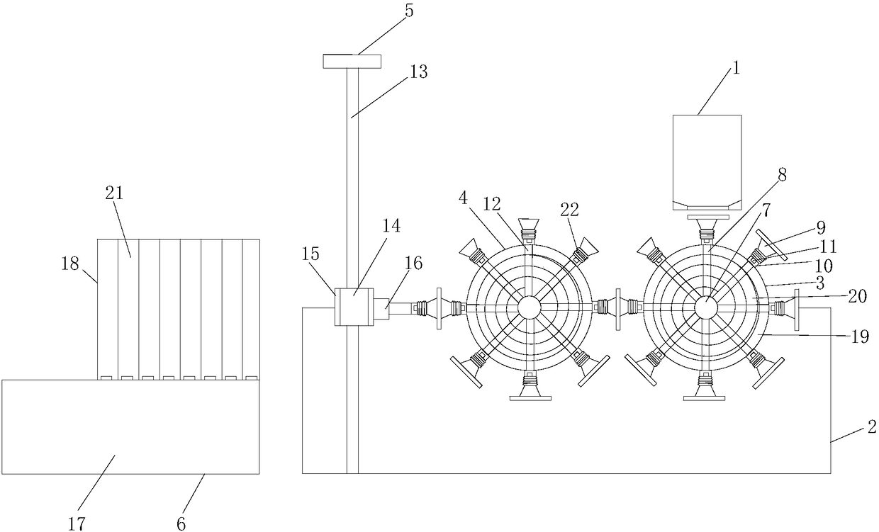
[0013] refer to figure 1 , a silicon chip automatic cleaning inserting device of the present invention, comprising a lower hopper 1, a cleaning tank 2, a material receiving cleaner 3, a turning cleaner 4, a transfer inserter 5, and an inserting rack 6, the lower hopper 1 It is arranged directly above the cleaning tank 2, and a material receiving cleaner 3 is arranged directly below the lower hopper 1, and the material receiving cleaner 3 includes a rotating wheel 7, a material receiving column 8, a material suction cup 9, and a vacuum valve 10 . Material sensor 11, the rotating wheel 7 is arranged in the cleaning tank 2, a number of material receiving columns 8 are evenly arranged around the rotating wheel 7, and a vacuum valve 10 is arranged at the outermost end of the material receiving column 8, The top of the vacuum valve 10 is equipped with a suction cup 9, the bottom of the suction cup 9 is provided with a material sensor 11, and the turning cleaner 4 is arranged on the ...


PUM


Abstract

The invention discloses automatic silicon chip insertion equipment with a cleaning function. The automatic silicon chip insertion equipment includes a discharge hopper, a cleaning tank, a material receiving cleaner, a turn-over cleaner, a chip transfer and insertion device and a chip insertion rack. The automatic silicon chip insertion equipment with a cleaning function can enable chip insertion of silicon wafers to be performed automatically, reduces artificial participation, improves chip insertion quality and efficiency, and the silicon chips can be turned over to be cleaned, thereby ensuring cleanliness and tidiness, and facilitating subsequent production.

Description

【Technical field】 [0001] The invention relates to the technical field of silicon wafer production, in particular to the technical field of automatic silicon wafer insertion equipment. 【Background technique】 [0002] Since the beginning of the 21st century, global energy consumption has risen sharply, and traditional fossil energy has been increasingly exhausted. Energy issues and environmental issues have gradually become two major issues of global concern. Under the pressure of sustainable development, major countries have listed the solar photovoltaic industry as the focus of the development and utilization of renewable energy. Silicon wafers are made of silicon rods by cutting and degumming. After the degumming is completed, the silicon wafers need to be divided into pieces, and then the pieces are inserted into the flower basket, and then subsequent cleaning and other processes are performed; in the prior art, the silicon wafers are The steps of slicing and inserting in...

Claims


Application Information

Patent Timeline
Patent Type & Authority Applications(China)
IPC IPC(8): H01L21/67H01L21/677H01L31/18
CPCH01L31/1876H01L21/67057H01L21/67781Y02P70/50
Inventor 马建国
Owner 浙江岐达科技股份有限公司
Why Eureka
Try Eureka