A medium array switch

An array switch and medium technology, which is applied in the direction of instruments, optics, electrical components, etc., can solve the problem that semiconductor switches are susceptible to electromagnetic interference, and achieve the effects of stable chemical properties, good acid and alkali resistance, and good anti-interference characteristics

Active Publication Date: 2020-05-19
HUAZHONG UNIV OF SCI & TECH
View PDF1 Cites 0 Cited by
  • Summary
  • Abstract
  • Description
  • Claims
  • Application Information

AI Technical Summary

Problems solved by technology

[0004] In view of the above defects or improvement needs of the prior art, the present invention provides a dielectric array switch, the purpose of which is to use the change of the photonic bandgap to control the transmission of the specified band to control the on-off of the signal, and to solve the problem that the existing semiconductor switch is vulnerable to electromagnetic interference. Interfering technical issues

Method used


Image

  • A medium array switch
  • A medium array switch
  • A medium array switch

Examples


Embodiment 1

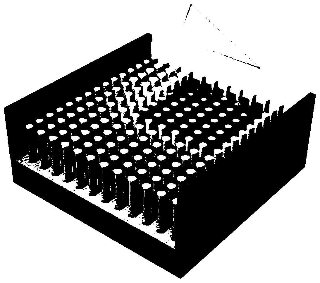
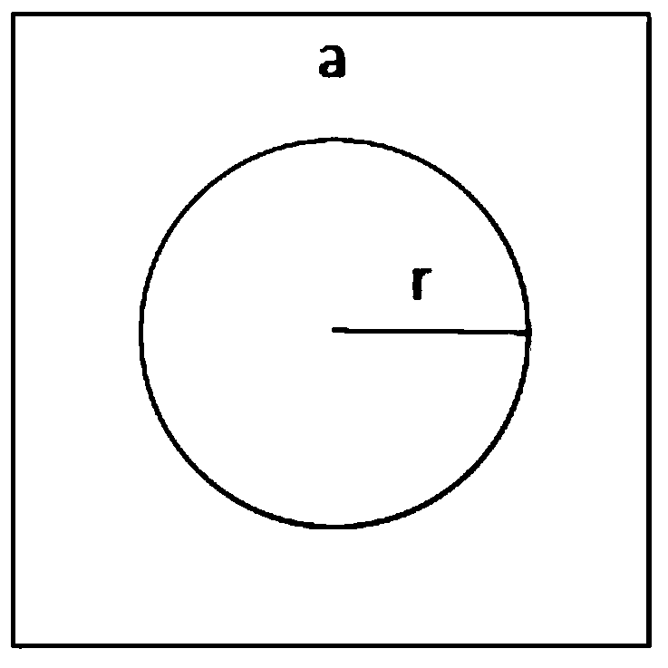
[0031] The dielectric array switch provided in Embodiment 1 is suitable for applications in the 20 GHz band, that is, the radar K-band; the length a of the array unit is 6 mm; the radius of the dielectric column is set to 2.5 mm.

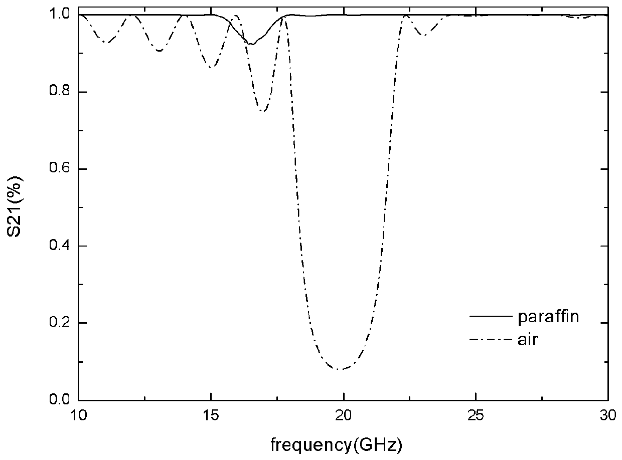
[0032] refer to figure 2 , is the effect diagram of transmittance at 20GHz provided by Example 1 of the present invention. When the structure is filled with paraffin wax, the transmittance at 20GHz frequency is as high as 99.9%, and electromagnetic waves pass through almost completely; When filling the medium, the transmittance is below 8.1%, and the electromagnetic wave is blocked and cannot pass through. Therefore, as the filling melts, the filling between the medium columns changes, and the propagation state of the electromagnetic wave in it also changes, realizing the switch function.

Embodiment 2

[0034] The dielectric array switch provided in embodiment 2 is suitable for the application of the 1550nm wave band; the length a of the array unit is set to 0.45um, and the radius r of the dielectric column is set to 0.16um; Simulation test.

[0035] refer to image 3 , is the effect diagram of the transmittance at 1550nm provided in Example 2. It can be seen that when the filling medium is paraffin, the transmittance at 1550nm is basically 1. It can be seen from the data that the transmittance is greater than 99.1%, and electromagnetic waves can pass through; while the paraffin melts When the dielectric pillars are filled with air, the transmittance is lower than 0.2%, the electromagnetic wave is basically unable to pass through, and the band gap is wider; in the two different filling media of paraffin and ambient air, the on-off state of the electromagnetic wave is different. This implements the switch function.

[0036] The dielectric array switch provided by the present...


PUM


Abstract

The invention belongs to the technical field of electromagnetic switches, and discloses a dielectric array switch. The switch comprises a pedestal, a medium array composed of M*N dielectric cylindersand arranged on the pedestal and heating components arranged at two sides of the dielectric array; the portion among the dielectric cylinders of the dielectric array is filled with a substance with alow melting point and strong liquidity after melting; when the dielectric array switch works, an incident wave is emitted from the direction parallel to the pedestal to heat the filler; when a heatingtemperature reaches the melting point of the filler, the filler is melted, the filler among the dielectric cylinders is environmental gas, so that dielectric constants of cylinder bodies of the dielectric cylinders are changed, transmissivity of the dielectric array switch to a electromagnetic wave of a certain wave band is changed, and the switch functions that the electromagnetic wave is allowed to pass through or is cut off are achieved; the dielectric array switch can prevent external electromagnetic waves from passing through, cannot be affected by external electromagnetic wave interference, and has good anti-interference performance, is applicable to communication wave bands and infrared wave bands, is extremely wide in application wavelength coverage, has significant switch performance, and is high in stability.

Description

technical field [0001] The invention belongs to the technical field of electromagnetic wave switch structures, and more particularly relates to a frequency-adjustable dielectric array switch. Background technique [0002] Microwave switch is an important part of microwave control circuit, and it is widely used in radar, satellite, communication and other communication fields. It is mainly used to control signal on-off and signal switching. [0003] In the early days, microwave switches were mainly realized through electromechanical structures; with the emergence of various new control devices, semiconductor switches gradually replaced electromechanical switches, such as GaAs field effect transistors, GaN high electron mobility transistors and Schottky barrier transistors, etc. Switches of new devices are constantly appearing. Due to the superior performance of semiconductor switches, the overall performance of microwave control circuits has been greatly improved. However, s...

Claims


Application Information

Patent Timeline
Patent Type & Authority Patents(China)
IPC IPC(8): G02B5/00H01P1/10
CPCG02B5/00H01P1/10
Inventor 龚荣洲牛晓燕王鲜祁冬
Owner HUAZHONG UNIV OF SCI & TECH
Why Eureka
Try Eureka