Liquid crystal display panel, display device and working method thereof

A technology of liquid crystal display panel and liquid crystal display device, applied in the field of display device and liquid crystal display panel, can solve the problems of low light transmittance, low energy utilization rate and high energy consumption of liquid crystal display, and achieve the effect of improving light output efficiency

Active Publication Date: 2021-01-26
BOE TECH GRP CO LTD
View PDF13 Cites 0 Cited by
  • Summary
  • Abstract
  • Description
  • Claims
  • Application Information

AI Technical Summary

Problems solved by technology

[0002] The existing liquid crystal display includes a liquid crystal display panel, a backlight source, and polarizers attached to the light-emitting side and the light-incoming side of the liquid crystal display panel. The liquid crystal display panel includes a color filter substrate, an array substrate, and an For the liquid crystal layer, since the transmittance of the color filter substrate, array substrate, and polarizer cannot reach 100%, the light energy emitted by the backlight will be greatly lost, and finally the light transmittance of the liquid crystal display can only reach about 5%, resulting in liquid crystal Low light transmittance of the display, high energy consumption, low energy utilization, etc.

Method used


Image

  • Liquid crystal display panel, display device and working method thereof
  • Liquid crystal display panel, display device and working method thereof
  • Liquid crystal display panel, display device and working method thereof

Examples


Embodiment Construction

[0052] In order to make the technical problems, technical solutions and advantages to be solved by the embodiments of the present invention clearer, the following will describe in detail with reference to the drawings and specific embodiments.

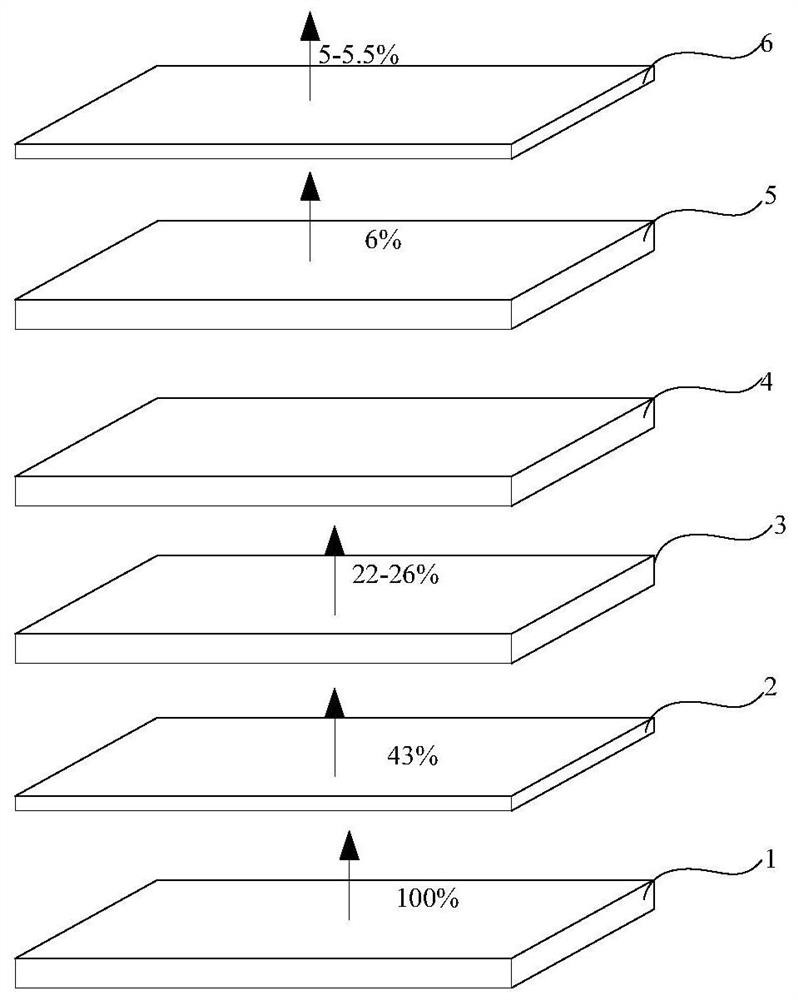
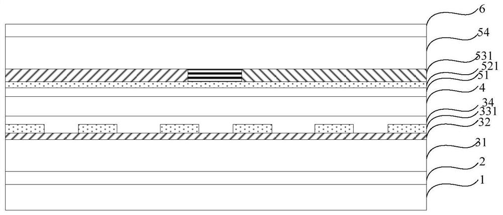
[0053] Such as figure 1 and figure 2 Shown is a schematic structural view of an existing liquid crystal display, the existing liquid crystal display includes a backlight 1, a lower polarizer 2, a first substrate 3, a liquid crystal layer 4, a second substrate 5 and an upper polarizer 6 arranged in sequence, the first The substrate 3 includes a base substrate 31 and a passivation layer 32 on the base substrate 31, a pixel electrode 331 and an alignment layer 34, and the second substrate 5 includes a base substrate 54 and a color filter unit 531 on the base substrate 54 , the common electrode 521 and the alignment layer 51 . Wherein, because the light transmittance of the lower polarizer 2, the first substrate 3, the liquid crystal l...


PUM

PropertyMeasurementUnit
thicknessaaaaaaaaaa
transmittivityaaaaaaaaaa

Abstract

The invention provides a liquid crystal display panel, a display device and a working method thereof, belonging to the field of display technology. The liquid crystal display panel includes a first substrate, a second substrate, and a liquid crystal layer between the first substrate and the second substrate. Each pixel area of ​​the liquid crystal display panel includes: a black matrix located on the second substrate, and the black matrix defines a The opening area; the light-trapping layer on the first substrate, the orthographic projection of the light-trapping layer on the second substrate falls into the black matrix; the light-reflecting layer between the liquid crystal layer and the black matrix; the first substrate and the second substrate Between the first electrode unit and the second electrode unit; after voltage is applied to the first electrode unit and the second electrode unit, the liquid crystal molecules in the corresponding regions of the liquid crystal layer can be deflected to form a microprism structure. The invention can improve the light extraction efficiency of the liquid crystal display device.

Description

technical field [0001] The invention relates to the field of display technology, in particular to a liquid crystal display panel, a display device and a working method thereof. Background technique [0002] The existing liquid crystal display includes a liquid crystal display panel, a backlight source, and polarizers attached to the light-emitting side and the light-incoming side of the liquid crystal display panel. The liquid crystal display panel includes a color filter substrate, an array substrate, and an For the liquid crystal layer, since the transmittance of the color filter substrate, array substrate, and polarizer cannot reach 100%, the light energy emitted by the backlight will be greatly lost, and finally the light transmittance of the liquid crystal display can only reach about 5%, resulting in liquid crystal The light transmittance of the display is low, the energy consumption is high, and the energy utilization rate is low. Contents of the invention [0003]...

Claims


Application Information

Patent Timeline
Patent Type & Authority Patents(China)
IPC IPC(8): G02F1/1335G02F1/13357
CPCG02F1/133512G02F1/133606G02F1/133607
Inventor 王海燕
Owner BOE TECH GRP CO LTD
Why Eureka
Try Eureka