Fingerprint sensing module and manufacturing method thereof
A manufacturing method and fingerprint technology, which is applied in semiconductor/solid-state device manufacturing, character and pattern recognition, instruments, etc., can solve the problems of complicated manufacturing process, large overall volume and thick thickness of the fingerprint packaging module, and achieve the effect of simple manufacturing method
- Summary
- Abstract
- Description
- Claims
- Application Information
AI Technical Summary
Problems solved by technology
Method used
Image

Examples
Embodiment Construction
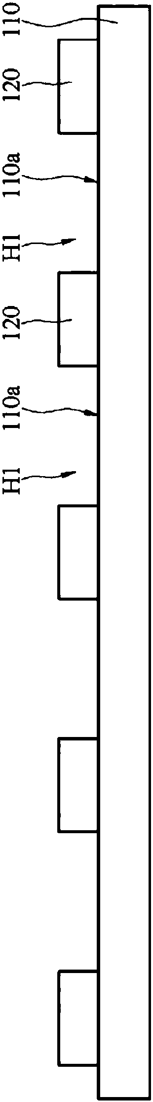
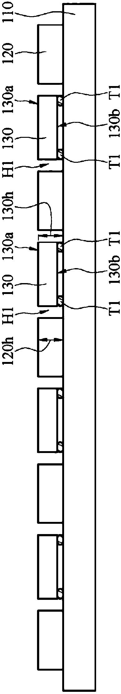
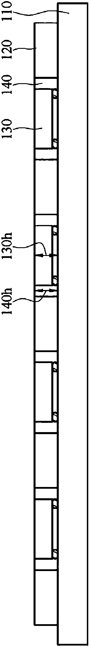
[0012] Figure 1A to Figure 1E Each is a schematic view of each step in the manufacturing method of the fingerprint sensing module according to an embodiment of the present invention. Please refer to Figure 1A to Figure 1E .
[0013] Firstly, a prefabricated layer 120 is formed on the circuit substrate 110 . see Figure 1A In detail, the molding material can be poured on the surface 110 a of the circuit substrate 110 through a mold (not shown), so that it is formed into a prefabricated layer 120 having at least one slot H1 . The slot H1 communicates with the upper surface and the lower surface of the prefabricated layer 120 , that is, the slot H1 can expose a part of the surface 110 a of the circuit substrate 110 . In addition, the width of the slot H1 may be greater than the size of the fingerprint sensing chip 130 so as to accommodate the fingerprint sensing chip 130 in subsequent processes. To avoid reducing the sensitivity of the fingerprint sensing chip 130 , in an em...
PUM
 Abstract
Description
Claims
Application Information
PatSnap Eureka turns technology decisions into work you can execute. Powered by our Innovation Knowledge Graph, it runs expert workflows across engineering, life sciences, materials and intellectual property. Get your review-ready output in minutes.


