Crystal oscillator

A crystal oscillator and crystal technology, applied in the field of circuits, can solve problems such as unfavorable crystal rapid start-up, MOS tube does not provide sufficient transconductance, etc., to achieve the effect of fast start-up, avoiding phase noise problems, and large transconductance

Active Publication Date: 2018-08-14
SHENZHEN GOODIX TECH CO LTD
View PDF8 Cites 12 Cited by
  • Summary
  • Abstract
  • Description
  • Claims
  • Application Information

AI Technical Summary

Problems solved by technology

However, there are some problems with the Pierce oscillator. The bias current of the two MOS tubes is affected by the gate-source voltage V of the MOS tubes. GS , and the sum of the gate-source voltages of the two MOS transistors is the power supply voltage V DD , therefore, if V DD When larger, the V of the MOS tube GS It is also bound to be large, which may lead to serious high-order effects. The problem is that although the power consumption of the MOS tube is large, in fact the MOS tube does not provide enough transconductance, which is not conducive to the rapid start-up of the crystal.

Method used


Image

  • Crystal oscillator
  • Crystal oscillator
  • Crystal oscillator

Examples


Embodiment Construction

[0035] The embodiments of the present application will be described below with reference to the accompanying drawings of the embodiments of the present application.

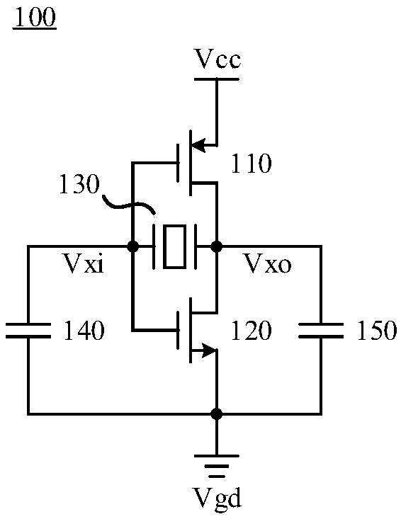
[0036] figure 1 is a schematic diagram of a typical structure of a crystal oscillator, such as figure 1 As shown, the crystal oscillator 100 includes a transistor 110 , a transistor 120 , a crystal 130 , a capacitor 140 and a capacitor 150 .

[0037] Wherein, the gate of the transistor 110 is connected to the gate of the transistor 120, and the drain of the transistor 110 is connected to the drain of the transistor 120, that is, the connection structure of the transistor 110 and the transistor 120 is an inverter, and the transistor 110 and the transistor 120 are used for The start and sustain oscillation of crystal 130 provides transconductance.

[0038] but, figure 1 The oscillator shown suffers from the following problem: the drain currents (or rather, the bias currents) of transistors 110 and 120 are contro...


PUM


Abstract

The present invention discloses a crystal oscillator. The crystal oscillator comprises: a crystal, an oscillating circuit, a first driving circuit, and a second driving circuit, wherein the oscillating circuit comprises a first oscillating transistor and a second oscillating transistor; the first oscillating transistor and the second oscillating transistor are used for providing transconductance for oscillation starting of the crystal and maintenance of oscillation; the first driving circuit is used for generating a stable reference current; and the second driving circuit is used for supplyingan operating voltage to the oscillating circuit, and enabling the operating current of the first oscillating transistor and the second oscillating transistor to be a stable current according to the reference current; and the operating voltage is used to control the first oscillating transistor and the second oscillating transistor to operate in a subthreshold region.

Description

technical field [0001] The embodiments of the present application relate to the circuit field, and more specifically, relate to a crystal oscillator. Background technique [0002] The Pierce oscillator (Pierce oscillator, or Pierce crystal oscillator) is a crystal oscillator using an inverter structure. Two metal oxide semiconductor field effect transistors (MetallicOxide Semiconductor Field Effect Transistor, MOSFET) in the Pierce oscillator Both contribute to the transconductance, which is beneficial to reduce the power consumption required for sustaining oscillation. However, there are some problems with the Pierce oscillator. The bias current of the two MOS tubes is affected by the gate-source voltage V of the MOS tubes. GS , and the sum of the gate-source voltages of the two MOS transistors is the power supply voltage V DD , therefore, if V DD When larger, the V of the MOS tube GS It is also bound to be large, which may lead to serious high-order effects. The proble...

Claims


Application Information

Patent Timeline
Patent Type & Authority Applications(China)
IPC IPC(8): H03B5/36H03B5/06H03B5/04
CPCH03B5/04H03B5/06H03B5/366H03B5/364H03B5/1228H03B5/24H03K3/02
Inventor 张孟文
Owner SHENZHEN GOODIX TECH CO LTD
Why Eureka
Try Eureka