Embedded-copper-block printed circuit board and manufacture method thereof

A technology for printed circuit boards and manufacturing methods, which is applied in the fields of printed circuits, printed circuits, multilayer circuit manufacturing, etc., can solve the problems of limited improvement of the overall heat dissipation performance of the circuit board, poor heat dissipation effect of the circuit board, etc., and achieve easy solution Cracking, good heat dissipation effect, and firm structure

Inactive Publication Date: 2018-08-17
KINWONG ELECTRONICS TECH LONGCHUAN
View PDF7 Cites 16 Cited by
  • Summary
  • Abstract
  • Description
  • Claims
  • Application Information

AI Technical Summary

Problems solved by technology

[0004] For this reason, the technical problem to be solved by the present invention is that the heat dissipation effect of the circuit board produced by the existing method of manufacturing the circuit board with buried copper blocks is not good, and it can only dissipate heat locally, and has a limited effect on improving the overall heat dissipation performance of the circuit board. Buried copper block printed circuit board with improved overall heat dissipation effect of circuit board and manufacturing method thereof

Method used


Image

  • Embedded-copper-block printed circuit board and manufacture method thereof

Examples


Embodiment 1

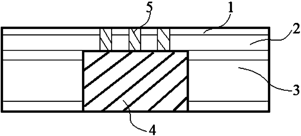
[0032] This embodiment provides a buried copper block printed circuit board, which is as follows figure 1 As shown, the top circuit layer 1, the prepreg layer 2 and the bottom circuit layer 3 are arranged sequentially from top to bottom, wherein the top circuit layer 1 is a copper foil layer with a circuit pattern, and its thickness is HOZ, and the bottom circuit layer Layer 3 is formed by cross-lamination of multi-layer PCB core boards with circuit patterns and prepregs (a prepreg is arranged between every two core boards). In this embodiment, the bottom circuit layer 3 is 4 layers, that is, It contains four layers of core boards and three layers of prepreg, and the thickness of the bottom circuit layer 3 is 0.2mm. And the material of the prepreg in the bottom circuit layer 3 is the same as that of the prepreg layer 2, the resin content is 68%, and the thickness of the prepreg layer 2 is 0.076mm.

[0033] The bottom circuit layer 3 is provided with an accommodation groove, t...

Embodiment 2

[0035] This embodiment provides a buried copper block printed circuit board, which is as follows figure 1 As shown, the top circuit layer 1, the prepreg layer 2 and the bottom circuit layer 3 are arranged sequentially from top to bottom, wherein the top circuit layer 1 is a copper foil layer with a circuit pattern, and its thickness is 1OZ, and the bottom circuit layer Layer 3 is formed by cross-lamination of multilayer PCB core boards and prepregs with circuit patterns (a prepreg is arranged between every two core boards). In this embodiment, the bottom circuit layer 3 is 20 layers, that is, It contains 20 layers of core boards and 19 layers of prepregs, and the thickness of the bottom circuit layer 3 is 6mm. And the material of the prepreg in the bottom circuit layer 3 is the same as that of the prepreg layer 2, the resin content is 75%, and the thickness of the prepreg layer 2 is 0.13 mm.

[0036] The bottom circuit layer 3 is provided with an accommodation groove, the acc...

Embodiment 3

[0038] This embodiment provides a buried copper block printed circuit board, which is as follows figure 1 As shown, the top circuit layer 1, the prepreg layer 2 and the bottom circuit layer 3 are arranged sequentially from top to bottom, wherein the top circuit layer 1 is a copper foil layer with a circuit pattern, and its thickness is 1OZ, and the bottom circuit layer Layer 3 is formed by cross-lamination of multi-layer PCB core boards and prepregs with circuit patterns (a prepreg is arranged between every two core boards). In this embodiment, the bottom circuit layer 3 is 10 layers, that is, It contains 10 layers of core boards and 9 layers of prepregs, and the thickness of the bottom circuit layer 3 is 3mm. Moreover, the material of the prepreg in the bottom circuit layer 3 is the same as that of the prepreg layer 2, the resin content is 70%, and the thickness of the prepreg layer 2 is 0.1 mm.

[0039]The bottom circuit layer 3 is provided with an accommodation groove, the...


PUM


Abstract

The invention discloses an embedded-copper-block printed circuit board, comprising a top wire layer, a prepreg layer and a bottom wire layer which are arranged in sequence; the bottom wire layer is provided with a receiving cavity; a radiating copper block is arranged in the receiving cavity; the top wire layer is provided with blind holes; the bottoms of the blind holes are connected with the radiating copper block. The radiating copper block is embedded in the circuit board, the top wire layer is connected with the radiating copper block via the blind holes, and a device may be welded directly to the laser blind holes and the radiating copper block such that a radiating substrate has greatly improved radiating and heat-conducting effects; the printed circuit board is applicable to heat dissipation for high-power devices; the printed circuit board is connected with the radiating copper block via the blind holes so that heat of the high-power devices may be dissipated in time, and thestability and reliability of the high-power devices are improved. The invention also discloses a method of manufacturing the embedded-copper-block printed circuit board. The manufacturing method is simple, the conditions are mild, and the manufactured printed circuit board has good radiating effect and good structural stability and rarely cracks.

Description

technical field [0001] The invention belongs to the technical field of printed circuit board production, and in particular relates to a high heat dissipation buried copper block printed circuit board and a manufacturing method thereof. Background technique [0002] With the continuous development of electronic devices towards intelligence, miniaturization and portability, the power density of electronic devices is increasing. The electric energy consumed by electronic devices during operation is mostly converted into heat except for some useful work. , The heat causes the internal temperature of the components to rise rapidly. If the heat is not dissipated in time, the continuous heating of electronic components will lead to quality degradation and even failure due to overheating. For electronic components with large heat generation, corresponding heat dissipation design is required, such as using metal substrates to make circuit boards, welding metal substrates on circuit b...

Claims


Application Information

Patent Timeline
Patent Type & Authority Applications(China)
IPC IPC(8): H05K1/02H05K3/46
CPCH05K1/0204H05K3/46H05K2201/10416
Inventor 沙伟强谭小林张军
Owner KINWONG ELECTRONICS TECH LONGCHUAN
Why Eureka
Try Eureka