Method for adjusting uniformity of ion milling

A uniformity and ion milling technology, applied in discharge tubes, electrical components, circuits, etc., can solve the problem that small-sized ion sources cannot meet wafer cleaning and other problems, and achieve the effects of saving procurement costs, stabilizing uniformity, and improving economic benefits.

Active Publication Date: 2018-08-21
NO 55 INST CHINA ELECTRONIC SCI & TECHNOLOGYGROUP CO LTD
View PDF6 Cites 3 Cited by
  • Summary
  • Abstract
  • Description
  • Claims
  • Application Information

AI Technical Summary

Problems solved by technology

[0003] The purpose of the present invention is to solve the problem that the small-sized ion source cannot satisfy the wafer cleaning problem in the existing deposition chamber, and to invent a method for adjusting the uniformity of ion milling, so as to realize the maximum utilization of the small-sized cylindrical ion source, so that it can Meets ion milling requirements for existing deposition chambers

Method used


Image

  • Method for adjusting uniformity of ion milling
  • Method for adjusting uniformity of ion milling
  • Method for adjusting uniformity of ion milling

Examples


Embodiment Construction

[0017] The present invention will be further described below in conjunction with the accompanying drawings and embodiments.

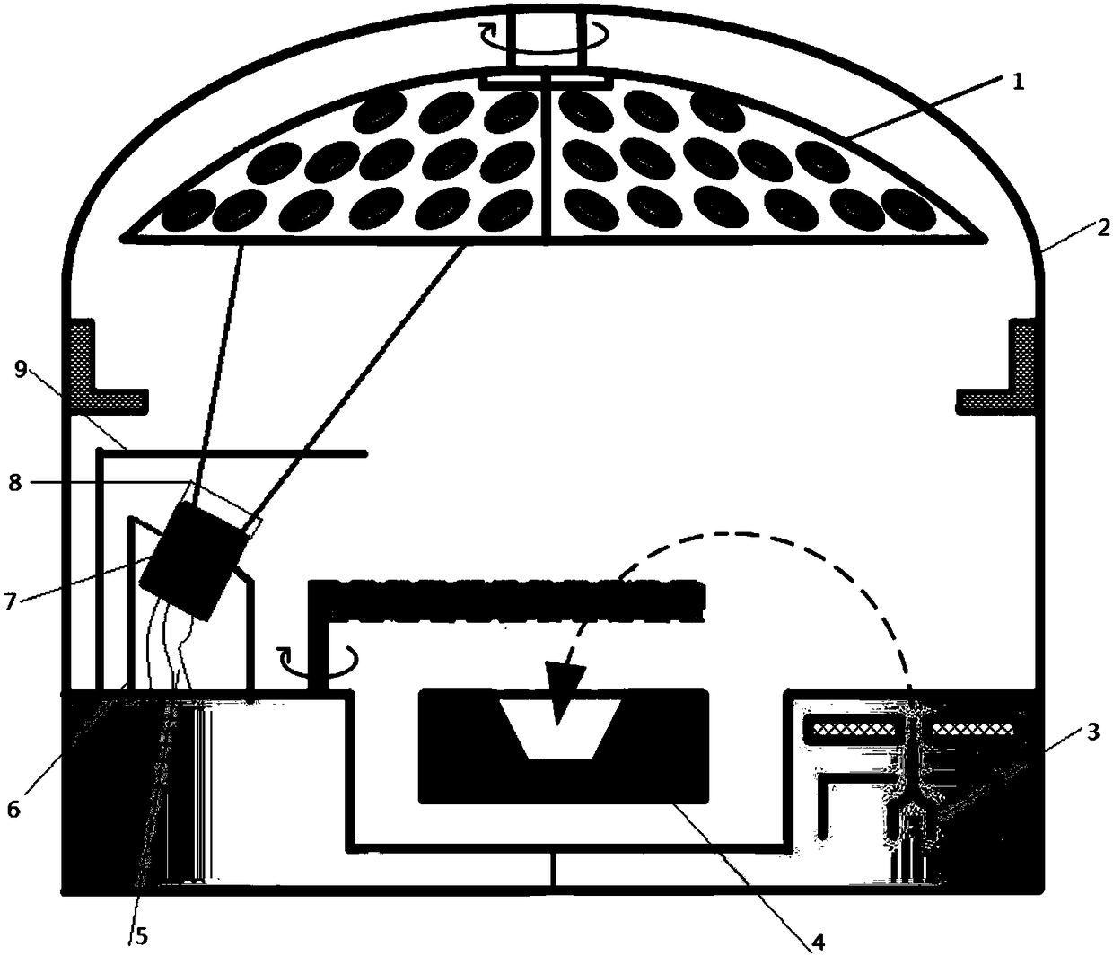
[0018] Such as Figure 1-5 shown.

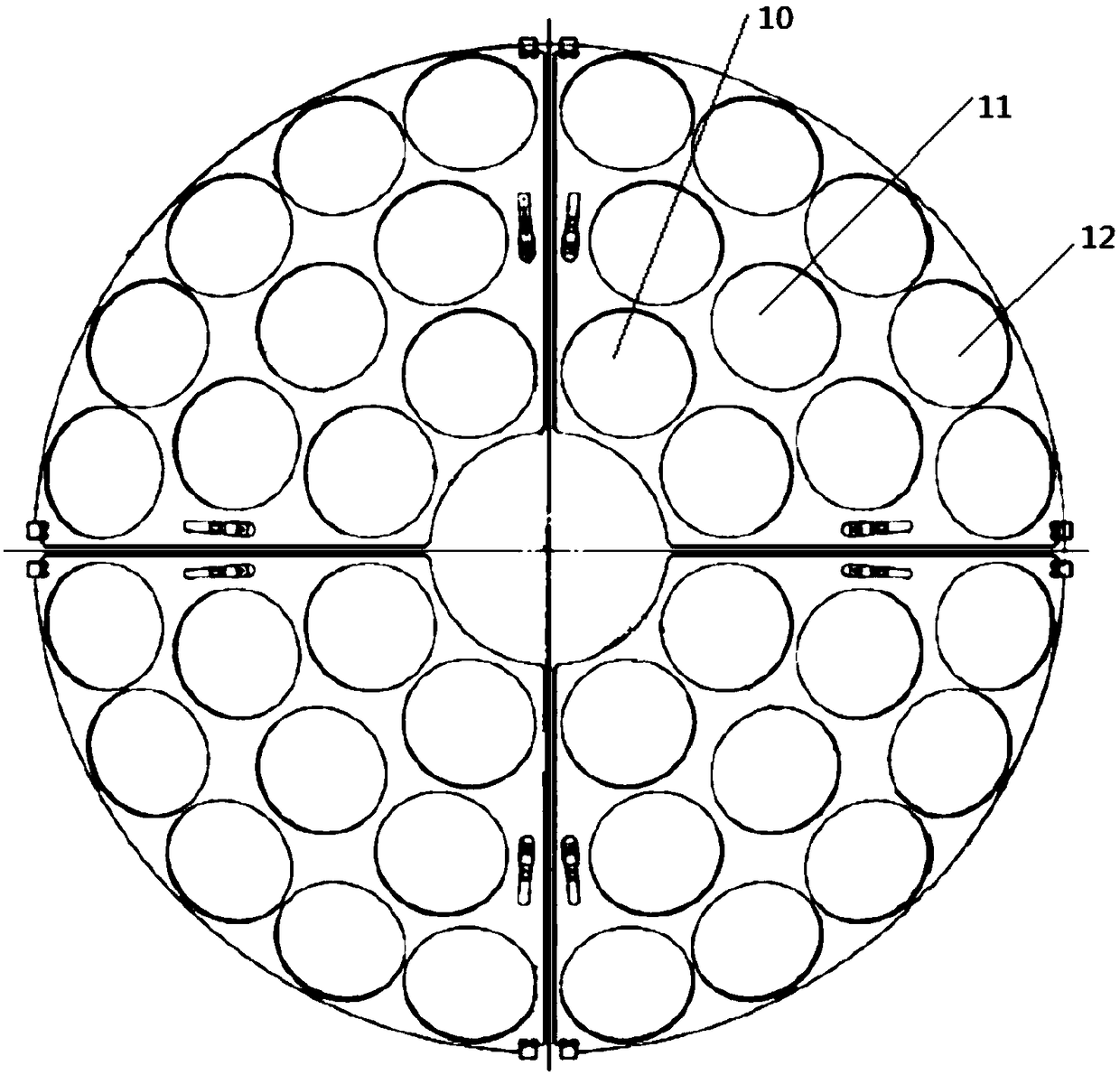
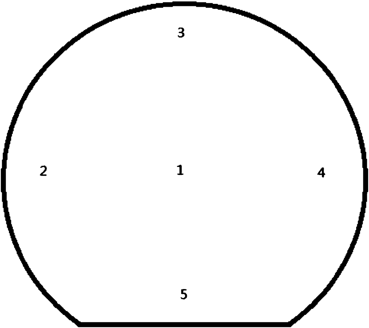
[0019] A method to adjust the uniformity of ion milling, first of all Figure 5 The ion milling source 7 shown is installed on an ion milling fixed bracket 6 with adjustable height and angle, and secondly, a uniformity baffle 8 is added outside the graphite grid 16 of the ion milling source 7; the ion milling source 7 is tilted The adjustment of angle, height and the function of uniformity baffle 8 realize the planetary disc ( figure 2 ) The ion milling uniformity of the wafers on the middle circle 11 and the outer circle 12 meets the uniformity within the wafer, between wafers and between wafer batches ≤ 10%, and at the same time ensures that the ion milling speed is greater than 0.9 nm / min. Wherein the shape of the through hole of the uniformity baffle plate 8 is a corrected fan shape, such as Figure 4 . The ...


PUM


Abstract

The invention relates to a method for adjusting the uniformity of ion milling, which is characterized in that the ion milling uniformity of wafers on a planetary disk middle ring 11 and a planetary disk outer ring 12 through adjusting the height and inclination angle of a cylindrical ion source and adding a uniform baffle. The method not only stabilizes the uniformity of ion milling, but also improves the productivity and the utilization ratio of equipment and meets the requirements of process production.

Description

technical field [0001] The present invention relates to a physical vapor deposition technology, especially a deposition technology used in semiconductor metallization process, in particular to a method for adjusting the uniformity of ion milling. Background technique [0002] Vacuum evaporation technology belongs to the method of physical vapor deposition film formation. It has the advantages of simple operation, high evaporation rate and good anisotropy. It is widely used in scientific research and production. In the micro-nano semiconductor manufacturing process, the general substrate material will have a thin oxide layer when it is exposed for a long time. Using plasma milling to remove this oxide layer will help to increase the adhesion of the metal and reduce the oxide layer. Effects on metal-to-semiconductor material contact. Usually the equipment will provide an ion source with an ion milling rate > 0.9nm / min, uniformity within a chip, between chips, and between b...

Claims


Application Information

Patent Timeline
IPC IPC(8): H01J37/30H01J37/32
CPCH01J37/305H01J37/32366
Inventor 殷履文夏久龙解晗
Owner NO 55 INST CHINA ELECTRONIC SCI & TECHNOLOGYGROUP CO LTD
Why Eureka
Try Eureka