
Surface mounting type diode

A diode and SMD technology, applied in the field of SMD diodes, can solve problems such as poor optical performance, achieve high refractive index, reduce energy consumption, improve light extraction efficiency and photoelectric replacement efficiency

Pending Publication Date: 2018-08-28
HEYUAN FUYU OPTOELECTRONICS TECH CO LTD
View PDF0 Cites 5 Cited by
  • Summary
  • Abstract
  • Description
  • Claims
  • Application Information

AI Technical Summary

Problems solved by technology

[0005] In order to overcome the deficiencies of the prior art, the purpose of the present invention is to provide a chip diode, which can solve the problem of poor optical performance caused by the planar structure of the packaging structure of semiconductor products in the prior art

Method used


Image

  • Surface mounting type diode
  • Surface mounting type diode
  • Surface mounting type diode

Examples


Embodiment

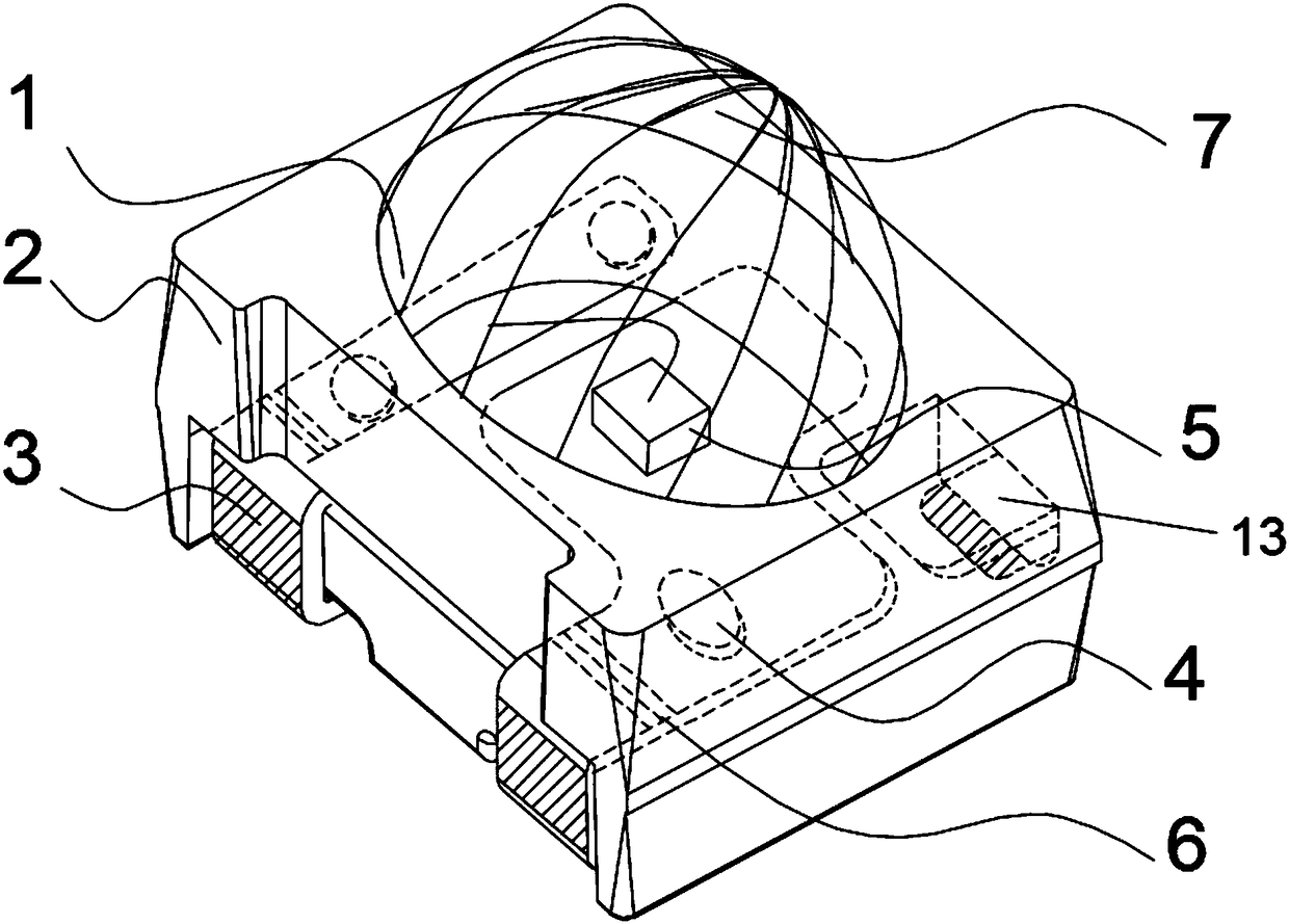
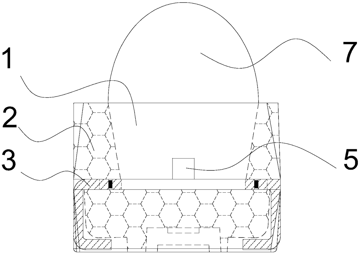
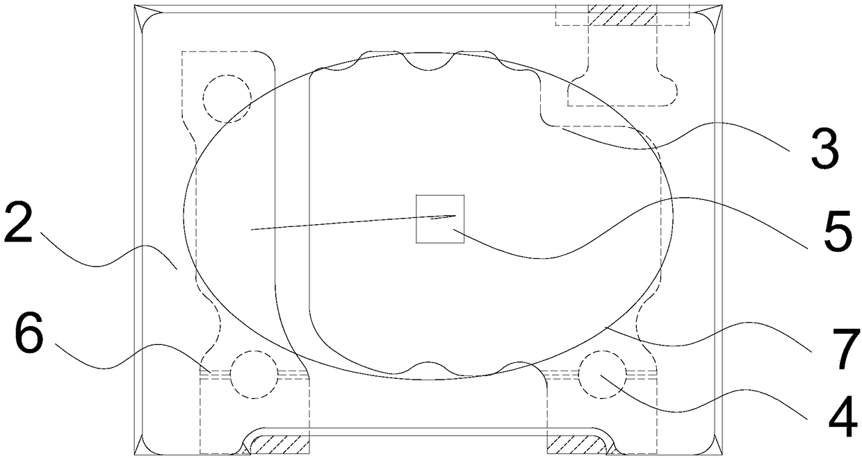
[0047] like Figure 1-6, the present invention provides a chip diode, which is improved on the existing planar packaging structure of semiconductor products. That is to say, the concave reflective groove 1 is injected at the position where the light source is fixed in the original planar package structure-package case 2, and the chip is placed on the bottom of the reflective groove 1, so that the light emitted / received by the chip can pass through the smooth surface. The inner wall of the reflective groove 1 performs concentrated reflection, thereby improving light extraction efficiency and photoelectric conversion efficiency, and reducing energy consumption. That is to say, a concave reflection groove 1 in the plastic casing 2 is used for placing the chip 5 . The chip 5 here may be devices such as visible light / infrared / ultraviolet emitting wafers, photoelectric receiving diodes, and ICs. In addition, the reflection groove 1 is, for example, bowl-shaped, cup-shaped, ellipti...


PUM


Abstract

The invention relates to a surface mounting type diode and particularly relates to a chip mounting type diode used for visible light / infrared light / ultraviolet light emission pipe products and photoelectric receiving pipe products. The chip mounting type diode comprises a plastic shell, a chip, a packaging colloid, metal leads and at least one metal lead frame, wherein a concave reflection grooveis formed in the plastic shell through injection molding, the chip is arranged at the bottom of the reflection groove, and the packaging colloid is arranged above the reflection groove and seals the reflection groove. The surface mounting type diode provided by the invention improves the light emission efficiency and the photovoltaic conversion efficiency, solves the problem of poor optical properties caused by adopting a planar structure for packaging in the prior art, and simultaneously can greatly reduce the energy consumption.

Description

technical field [0001] The invention relates to a chip type diode, in particular to a chip type diode used for visible light / infrared / ultraviolet emitting tubes and photoelectric receiving tube products. Background technique [0002] Packaging is to use a lead frame to carry the chip, use silver glue or metal connecting wires for internal and external electrical connections, and use colloid for protection and optical lens applications on the outside. Packaging is necessary for semiconductor devices to protect and increase optoelectronic performance. [0003] Most LED semiconductor devices on the market are packaged in pin-insert and surface-mount packages. Pin plug-in package: Use die-bonding glue to fix the chip on the metal bracket, and use metal wires to connect the electrodes. After realizing the electrical function connection, insert it into the molding cavity, inject liquid epoxy resin, and let the epoxy resin cure. , Release the LED from the mold cavity. Surface-mo...

Claims


Application Information

Patent Timeline
Patent Type & Authority Applications(China)
IPC IPC(8): H01L33/62H01L33/48H01L33/60H01L33/56
CPCH01L33/48H01L33/56H01L33/60H01L33/62
Inventor 赵志强
Owner HEYUAN FUYU OPTOELECTRONICS TECH CO LTD
Learn More