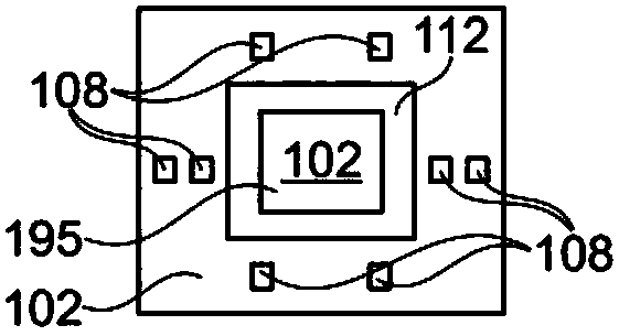
Patterned cover layer on base structure defining cavity and alignment marker
A technology for aligning marks and covering layers, which is applied in the fields of electric solid-state devices, semiconductor devices, multilayer circuit manufacturing, etc.
- Summary
- Abstract
- Description
- Claims
- Application Information
AI Technical Summary
Problems solved by technology
Method used
Image
Examples
Embodiment Construction
[0048] Before describing the exemplary embodiments in further detail with reference to the accompanying drawings, some basic considerations upon which the exemplary embodiments of the present invention are developed will be outlined.
[0049] According to an exemplary embodiment of the present invention, there is provided a component-embedded package with high accuracy. More specifically, an exemplary embodiment of the present invention provides a package or module with embedded electronics configured such that the entire registration chain becomes efficient and thus can be kept very small. manufacturing tolerances. By taking this measure, a high packing density can be achieved, allowing also a high degree or extensive functionality of the package in which the components are embedded.
[0050]An advantage achievable by exemplary embodiments of the present invention is high quality registration between cavities and components. Furthermore, during the laser cutting process of ...
PUM
 Abstract
Description
Claims
Application Information


