Flat panel detector and its preparation method

A flat-panel detector and planarization layer technology, applied in the field of flat-panel detectors and its preparation, can solve problems affecting product yield, affecting factory production capacity, and complicated preparation process, so as to reduce the use of MASK, high photoelectric conversion efficiency, The effect of high sensitivity

Active Publication Date: 2021-01-22
BOE TECH GRP CO LTD +1
View PDF6 Cites 0 Cited by
  • Summary
  • Abstract
  • Description
  • Claims
  • Application Information

AI Technical Summary

Problems solved by technology

[0002] Flat panel detectors, especially amorphous silicon diode flat panel detectors, are favored by a large number of customers due to their large size, high resolution, high sensitivity, and low noise. However, the traditional process of preparing flat panel detectors is through multiple masks (MASK ) process can be completed, the preparation process is more complicated, and the cost is higher, which greatly affects the production capacity of the factory, and will also affect the yield of the product
[0003] Therefore, the current flat panel detectors still need to be improved

Method used


Image

  • Flat panel detector and its preparation method
  • Flat panel detector and its preparation method
  • Flat panel detector and its preparation method

Examples


Embodiment Construction

[0022] Embodiments of the present invention are described in detail below. The embodiments described below are exemplary only for explaining the present invention and should not be construed as limiting the present invention. If no specific technique or condition is indicated in the examples, it shall be carried out according to the technique or condition described in the literature in this field or according to the product specification. The reagents or instruments used were not indicated by the manufacturer, and they were all commercially available conventional products.

[0023] The present invention is based on the following knowledge and findings of the inventors:

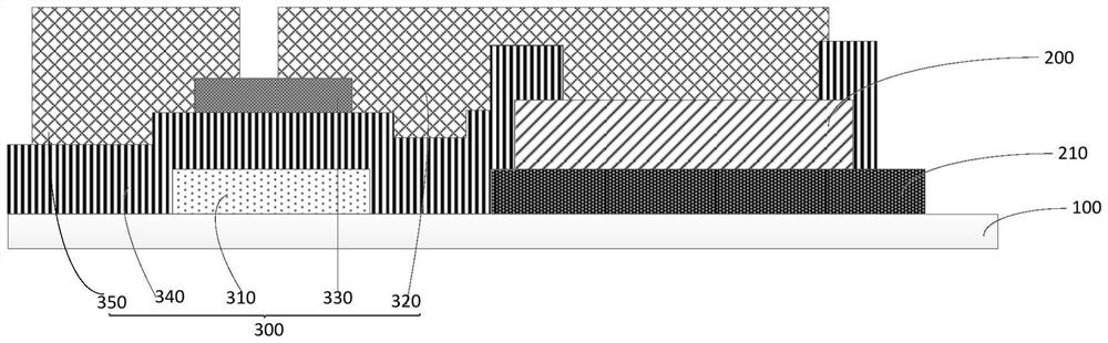
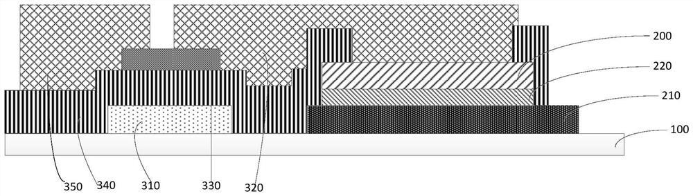
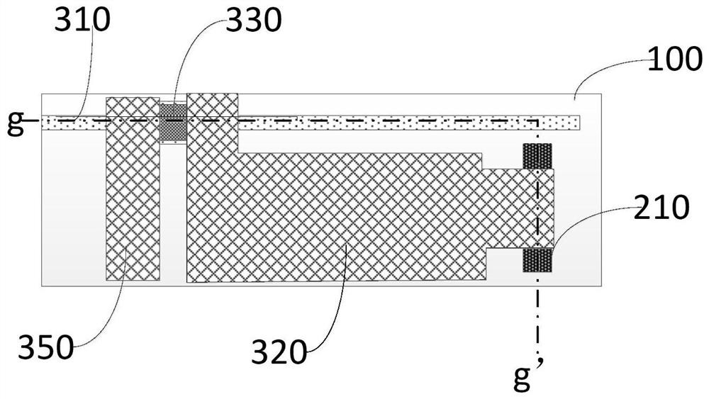
[0024] At present, the structure of the flat panel detector is relatively complicated. In the preparation process, the thin film transistor is usually prepared first, and then the photoelectric conversion film layer is prepared. The preparation steps are relatively cumbersome, and more times of MASK or more m...


PUM


Abstract

The invention provides a flat plate detector and a preparation method thereof. The flat plate detector comprises a substrate, a thin film transistor, a first electrode and a photoelectric conversion film layer. The thin film transistor is arranged on the first surface of the substrate. The first electrode is arranged on the first surface and on the same layer with the grid electrode of the thin film transistor. The photoelectric conversion film layer is arranged between the first electrode and the drain electrode of the thin film transistor, and is electrically connected with the first electrode and the drain electrode. The inventor finds that the flat plate detector is simple in structure, easy to achieve and quite thin; the grid electrode of the thin film transistor and the first electrode are arranged on the same layer, so the structure can be simplified and the technique processes are reduced; the photoelectric conversion film is arranged between the first electrode and the drain electrode, so the whole technique steps can be reduced and the yield of factories can be greatly improved; and meanwhile, the yield of the flat plate detector is quite high and can be prevented from being scratched during transmission or use processes.

Description

technical field [0001] The present invention relates to the technical field of photoelectric conversion, in particular to a flat panel detector and a preparation method thereof. Background technique [0002] Flat panel detectors, especially amorphous silicon diode flat panel detectors, are favored by a large number of customers due to their large size, high resolution, high sensitivity, and low noise. However, the traditional process of preparing flat panel detectors is through multiple masks (MASK ) process can be completed, the preparation process is more complicated, and the cost is higher, which greatly affects the production capacity of the factory, and also affects the yield rate of the product. [0003] Therefore, the current flat panel detectors still need to be improved. Contents of the invention [0004] The present invention aims to solve one of the technical problems in the related art at least to a certain extent. Therefore, an object of the present inventio...

Claims


Application Information

Patent Timeline
Patent Type & Authority Patents(China)
IPC IPC(8): H01L27/144H01L21/84
CPCH01L21/84H01L27/1443
Inventor 王凤涛张家祥王亮潘宗玮
Owner BOE TECH GRP CO LTD
Why Eureka
Try Eureka