Integrated circuit memory and forming method thereof, semiconductor integrated circuit device

A technology of integrated circuits and memory, which is applied in the field of semiconductor integrated circuits, and can solve problems such as resolution limitations of memory lithography equipment

Pending Publication Date: 2018-09-04
CHANGXIN MEMORY TECH INC
View PDF13 Cites 15 Cited by
  • Summary
  • Abstract
  • Description
  • Claims
  • Application Information

AI Technical Summary

Problems solved by technology

It can be seen that the size of the existing memory is not only limited by the resolution of the lithog

Method used


Image

  • Integrated circuit memory and forming method thereof, semiconductor integrated circuit device
  • Integrated circuit memory and forming method thereof, semiconductor integrated circuit device
  • Integrated circuit memory and forming method thereof, semiconductor integrated circuit device

Examples


Embodiment 2

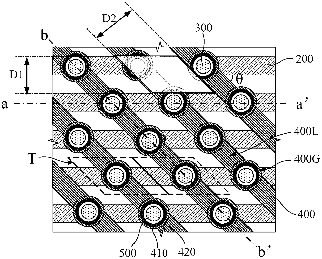
[0164] Figure 4 It is a schematic flow chart of the forming method of the memory in Embodiment 2 of the present invention, refer to Figure 4 As shown, in this embodiment, the forming method of the memory includes:

[0165] Step S100, providing a substrate, and forming a plurality of bit lines on the substrate, the bit lines extending along a first direction;

[0166] Step S200, forming a plurality of active pillars on the bit line, the bottom ends of the active pillars are connected to the bit lines, and the cross-sectional size of the bottom ends of the active pillars is a cross-sectional dimension smaller than the top end of the active pillar such that the bottom end is recessed relative to the top end;

[0167] Step S300, forming a plurality of word lines on the substrate, the word lines extending along the second direction, the word lines are integrally connected in the extending direction and configured with a plurality of upright gate transistors, the The gate trans...


PUM

PropertyMeasurementUnit
Width sizeaaaaaaaaaa

Abstract

The invention provides an integrated circuit memory, a forming method thereof and semiconductor integrated circuit device. The integrated circuit memory adopts a vertical memory transistor formed by active cylinders which are vertically arranged on a substrate, thereby being conductive to reducing unit configuration size of the vertical memory transistor on the substrate, and being capable of further reducing the size of the memory; in addition, the vertical memory transistors of a vertical structure have better arrangement flexibility, for example, hexagonal dense arrangement of a plurality of the vertical memory transistors can be realized to increase the arrangement density of memory cells in the memory. Moreover, the active cylinders adopted in the integrated circuit memory are of a structure with wide upper part and narrow lower part, such that the portion surrounding the bottom end parts of the active cylinders of a word line have large thickness, thereby being conductive to improving the performance of the vertical memory transistor.

Description

technical field [0001] The invention relates to the technical field of semiconductor integrated circuits, in particular to an integrated circuit memory and its forming method, and a semiconductor integrated circuit device. Background technique [0002] Semiconductor integrated circuit devices are getting smaller and smaller, making them more compact for mobile computing applications, consuming less energy and extending battery life between charges. And, with the reduction of the size of the semiconductor device, the circuit density can be increased correspondingly, so that the semiconductor device can have more powerful computing capability. [0003] However, today's technological development has been limited by the resolution of the lithography equipment available at the time. Specifically, the size of semiconductor integrated circuit devices, such as the minimum size of line width CD (Critical Dimension) and line distance S (spaces), depends on the resolution capability o...

Claims


Application Information

Patent Timeline
IPC IPC(8): H01L27/108H01L29/10H01L29/78H01L21/336H01L21/8242
CPCH01L29/1037H01L29/66666H01L29/7827H10B12/30H10B12/09
Inventor 不公告发明人
Owner CHANGXIN MEMORY TECH INC
Why Eureka
Try Eureka