Microstrip antenna, preparation method thereof and electronic equipment

A microstrip antenna and feeder technology, applied in the directions of antennas, resonant antennas, electrical short antennas, etc., can solve the problems of inability to directly connect external excitation sources, inability to accurately align the dielectric substrate, and deteriorate the performance of microstrip antennas. Mass production, low cost, easy to achieve effects

Active Publication Date: 2018-09-04
BOE TECH GRP CO LTD
View PDF7 Cites 21 Cited by
  • Summary
  • Abstract
  • Description
  • Claims
  • Application Information

AI Technical Summary

Problems solved by technology

Liquid crystal can realize the function of beam scanning, but because the thickness of the liquid crystal cell is only on the order of microns, it cannot be directly connected to an external excitation source. Causes losses in physical contact between metals
Mor

Method used


Image

  • Microstrip antenna, preparation method thereof and electronic equipment
  • Microstrip antenna, preparation method thereof and electronic equipment
  • Microstrip antenna, preparation method thereof and electronic equipment

Examples


Embodiment Construction

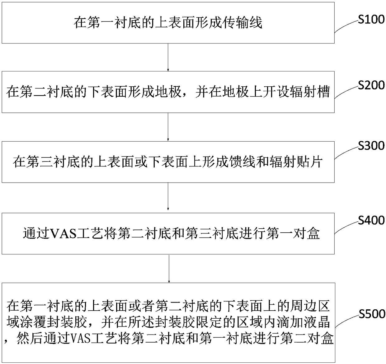
[0015] Embodiments of the present invention are described in detail below. The embodiments described below are exemplary only for explaining the present invention and should not be construed as limiting the present invention. If no specific technique or condition is indicated in the examples, it shall be carried out according to the technique or condition described in the literature in this field or according to the product specification. The reagents or instruments used were not indicated by the manufacturer, and they were all commercially available conventional products.

[0016] The present invention is based on the following knowledge and findings of the inventors:

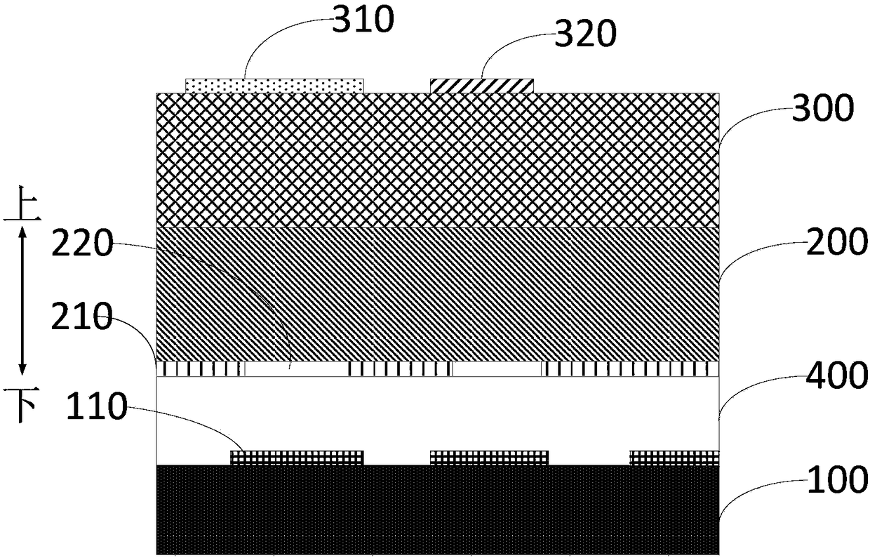
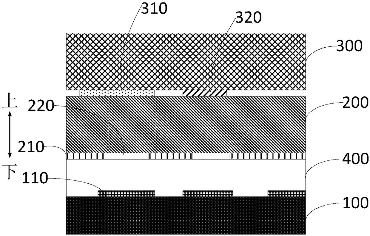
[0017] At present, when preparing a microstrip antenna, a patterned metal thin layer is usually deposited on two opposite surfaces of a substrate, one side is used as a ground electrode, and the other side is formed into a patch as a radiation antenna unit. The appearance of the liquid crystal antenna has ch...


PUM

PropertyMeasurementUnit
Thicknessaaaaaaaaaa

Abstract

The invention provides a microstrip antenna, a preparation method thereof and electronic equipment. The microstrip antenna comprises a first substrate, a second substrate and a third substrate which are sequentially stacked from bottom to top, a transmission line arranged on the upper surface of the first substrate, a ground electrode arranged on the lower surface of the second substrate and having a radiation slot, a liquid crystal layer arranged between the first substrate and the second substrate, and a feeder line and a radiation patch arranged on the upper surface or the lower surface ofthe third substrate, wherein orthographic projection of the feeder line, the radiation patch and the transmission line at least partially overlaps the orthographic projection of the radiation slot onthe first substrate, the transmission line and the ground electrode form a signal transmission line, the signal transmission line and the liquid crystal layer form a phase shifter, and the ground electrode, the transmission line, the feeder line and the radiation patch are arranged on the single-side surfaces of the different substrates respectively. The microstrip antenna has the advantages of simple preparation and low cost, is precise in alignment and has a high yield.

Description

technical field [0001] The invention relates to the technical field of semiconductor technology, in particular to a microstrip antenna, a preparation method thereof, and an electronic device. Background technique [0002] Microstrip antennas have the characteristics of light size, light weight, and easy conformability, and are usually prepared by printed circuit board (PCB) technology. Liquid crystals can realize the function of beam scanning, but because the thickness of the liquid crystal cell is only on the order of microns, it cannot be directly connected to an external excitation source. It will cause loss when the metal is in physical contact. Moreover, the dielectric substrate prepared by the PCB process cannot achieve accurate alignment with the liquid crystal cell, which will deteriorate the performance of the microstrip antenna. [0003] Therefore, the current microstrip antenna still needs to be improved. Contents of the invention [0004] The present inventi...

Claims


Application Information

Patent Timeline
IPC IPC(8): H01Q1/36H01Q1/38H01Q1/50H01Q13/08
CPCH01Q1/36H01Q1/38H01Q1/50H01Q13/08H01P1/184H01Q3/36H01Q9/0457H01Q9/0407
Inventor 方家李延钊王熙元刘宗民
Owner BOE TECH GRP CO LTD
Why Eureka
Try Eureka