Manufacturing method of multilayer printed board embedded resistor

A technology of multi-layer printed boards and embedded resistors, applied in directions including printed resistors, multi-layer circuit manufacturing, and printed electrical components, etc. problems, to achieve the effect of neat graphics edges, uniform thickness, and improved production efficiency and quality

Inactive Publication Date: 2018-09-04
陈长生
View PDF3 Cites 1 Cited by
  • Summary
  • Abstract
  • Description
  • Claims
  • Application Information

AI Technical Summary

Problems solved by technology

[0009] The technical problem to be solved by the present invention is to provide a method for making embedded resistors in multi-layer printed boards by screen printing resistor paste with simple process and reliable quality, which can produce embedded resistor patterns with high precision in position and size, and controllable resistance , to avoid problems such as uneven resistor edges, uneven thickness, and heavy resistance correction workload, etc., and a smaller square resistor size can be selected to reduce the size of the resistor pattern while meeting the resistance value requirements, thereby increasing the wiring density. It meets the requirements of modern electronic products, which are light, thin and short, and is especially suitable for the production of small IoT sensors and electronic products for microsystems in the future.

Method used


Image

  • Manufacturing method of multilayer printed board embedded resistor
  • Manufacturing method of multilayer printed board embedded resistor
  • Manufacturing method of multilayer printed board embedded resistor

Examples


Embodiment Construction

[0029] The present invention is further explained below in conjunction with embodiment. But the scope of protection of this patent is not limited to the specific implementation.

[0030] Implementation example

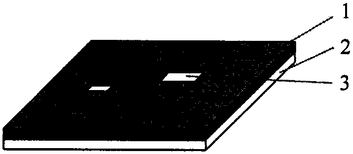
[0031] The multilayer printed board with embedded resistors produced in this example is a 4-layer printed board with dimensions 100mm×150mm×1.6mm embedded with 100 resistors with a resistance value of 2.8KΩ. The resistors are embedded in the second layer of the multilayer printed board. Before the inner layer board is processed to make the inner layer circuit, the embedded resistor is made on the inner layer board. It is necessary to etch and remove the copper foil embedded in the resistance part of the inner layer board, and then print the resistance paste with the required square resistance value on this part according to the design requirements, and then complete the embedded resistance after pre-baking, mechanical brushing and post-curing. Then, according to the...


PUM


Abstract

The present invention provides a manufacturing method of a multilayer printed board embedded resistor by using a screen printing resistor paste. The method comprises the following steps: in the manufacturing process of an inner layer board of a multilayer printed board, before the circuit(s) are manufactured on the inner layer board, required resistance patterns are etched on an inner layer boardcopper foil; the resistor paste of a prescribed square resistance value is subjected to screen printing on the resistance patterns; and after pre-drying, mechanical polish-brush and post curing, the other circuit patterns are manufactured to form the inner layer board embedded with resistor(s) of the specific resistance value. According to the method, the problems of irregular border and uneven thickness in a conventional screen printing resistor are avoided, the method is easy to operate, the resistance value is easy to control, the production efficiency and quality of the multilayer printedboard embedded resistor are improved, the assembly density is improved, and the production requirements of lightness, thinness, shortness and minimization of electronic products are satisfied.

Description

technical field [0001] The invention relates to the field of making special printed boards, including in the process of making inner layer boards of multilayer printed boards. Resistor pattern, and then screen-print the resistor paste with specified square resistance value on the resistor pattern, after pre-baking, mechanical grinding, post-curing and other circuit pattern production, to form a multi-layer printed board embedded with specific resistance value resistors Use the inner layer board, and then complete the inner layer board with embedded resistors and circuit patterns, together with other supporting inner layer boards and auxiliary bonding materials, make a multilayer printed board with embedded resistors according to the conventional multilayer printed board production process . [0002] The invention improves the precision of the resistance value of the embedded resistance made by screen printing resistance paste, reduces the workload of resistance value correcti...

Claims


Application Information

Patent Timeline
Patent Type & Authority Applications(China)
IPC IPC(8): H05K3/46H05K3/12H05K1/16
CPCH05K1/167H05K3/1216H05K3/1283H05K3/4641H05K2203/11
Inventor 陈长生
Owner 陈长生
Why Eureka
Try Eureka