Atomic beam microscope device

An atomic beam, atomic technology, applied in the field of atomic beam microscopy, can solve the problems of difficult processing, unsupported, insufficient atomic beam focusing effect, etc., and achieve the effect of suppressing diffraction, sharply focusing beam spot, and optimizing focusing effect.

CN108508047APending Publication Date: 2018-09-07JINHUA VOCATIONAL TECH COLLEGE
0 Cites 0 Cited by

Patent Information

Authority / Receiving Office
CN · China
Current Assignee / Owner
Publication Date
2018-09-07

Smart Images

  • Figure 1
    Figure 1
  • Figure 2
    Figure 2
  • Figure 3
    Figure 3
Patent Text Reader

Abstract

The invention relates to the technical field of microscopy for materials. The atomic beam microscope device comprises a gas storage tank, a gas pipe, a vacuum chamber formed by connection of a chamberI and a chamber II, an injector head, a shunt, a gas transmission window sheet, an atom diffraction plate, an atom diffraction plate through hole variety I, an atom diffraction plate through hole variety II, an atom diffraction plate through hole variety III, a detector I, a sample, a sample table, a computer, a detector II, an extraction opening I, a vacuum pump set I, an extraction opening II and a vacuum pump set II. According to the invention, for the atom diffraction plate, a series of through holes are adopted to replace the cyclic structure of a zone plate, the through holes are easierin processing than the cyclic structure without support of a standard fresnel zone plate, and the focusing effect of atomic beam current is optimized by selecting proper through hole diameter and through hole distribution, so as to obtain sharp focusing beam spots and inhibit diffraction of a higher order.
Need to check novelty before this filing date? Find Prior Art

Description

technical field

[0001] The invention relates to the field of microscopic technology for materials, in particular to an atomic beam microscopic device which uses atomic beams to scan the surface of a sample and has a specially designed atomic diffraction sheet. Background technique

[0002] In the field of microscopic technology, the existing electron microscope can only image conductive samples, and the electron beam emitted by the electron microscope is of high energy, which will cause some sensitive sample surfaces to be damaged by radiation. The atomic beam microscope can overcome the above defects and image fragile or insulating samples. It usually uses inert gas atoms as the emitting atoms. The energy of the atomic beam of the inert gas is very low and its chemical properties are very stable. Obtain an image of the surface of the sample. The working principle of the atomic beam microscope is: in a high vacuum, the free atomic flow passes through the nozzle and the aper...

Examples

Embodiment Construction

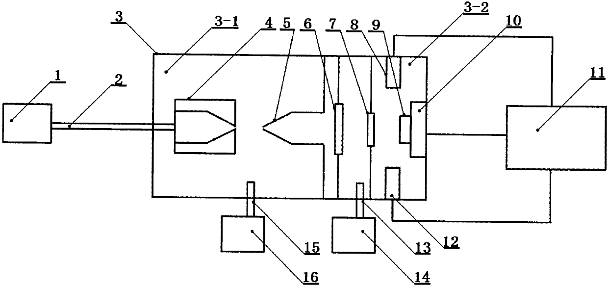
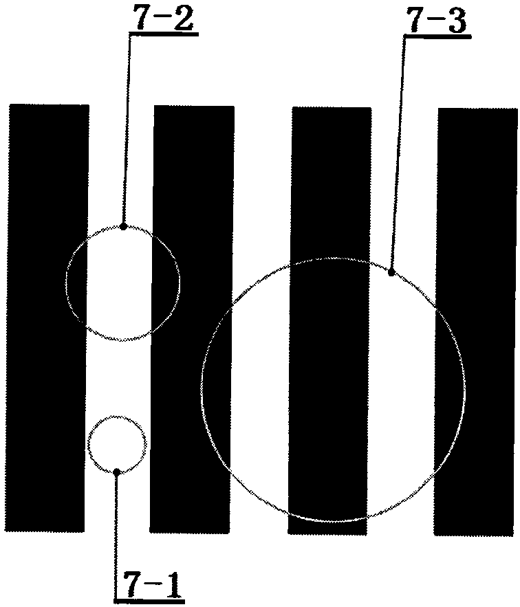
[0027] Such as figure 1It is a schematic diagram of the present invention, mainly comprising a gas storage tank (1), a gas pipe (2), a vacuum chamber (3) connected by a chamber body I (3-1) and a chamber body II (3-2), and a spray head ( 4), splitter (5), gas transmission window (6), atomic diffraction sheet (7), atomic diffraction sheet through hole type I (7-1), atomic diffraction sheet through hole type II (7-2), Type III (7-3) through hole of atomic diffraction sheet, detector I (8), sample (9), sample stage (10), computer (11), detector II (12), exhaust port I (13), Vacuum pump group I (14), suction port II (15), vacuum pump group II (16), the cavity I (3-1) and cavity II (3-2) are connected through a flow divider (5), and the cavity II(3-2) is connected to the vacuum pump group I(14) through the suction port I(13), and the cavity I(3-1) is connected to the vacuum pump group II(16) through the suction port II(15); the injection head (4) is located at In the cavity I (3-...