
Method for driving power semiconductor switches in H-bridge circuit

A technology of power semiconductor and driving method, which is applied to the conversion device of output power, the conversion of AC power input to DC power output, electrical components, etc.

Inactive Publication Date: 2018-09-07
DELTA ELECTRONICS SHANGHAI CO LTD
View PDF5 Cites 0 Cited by
  • Summary
  • Abstract
  • Description
  • Claims
  • Application Information

AI Technical Summary

Problems solved by technology

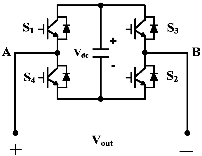
[0005] The invention provides a driving method of a power semiconductor switch in an H bridge circuit, which is used to solve how to reasonably drive the power semiconductor switch in the H bridge circuit in the process of outputting zero level in the multilevel converter in the prior art. Technical Problems of Power Semiconductor Switch Conduction

Method used


Image

  • Method for driving power semiconductor switches in H-bridge circuit
  • Method for driving power semiconductor switches in H-bridge circuit
  • Method for driving power semiconductor switches in H-bridge circuit

Examples


example 1

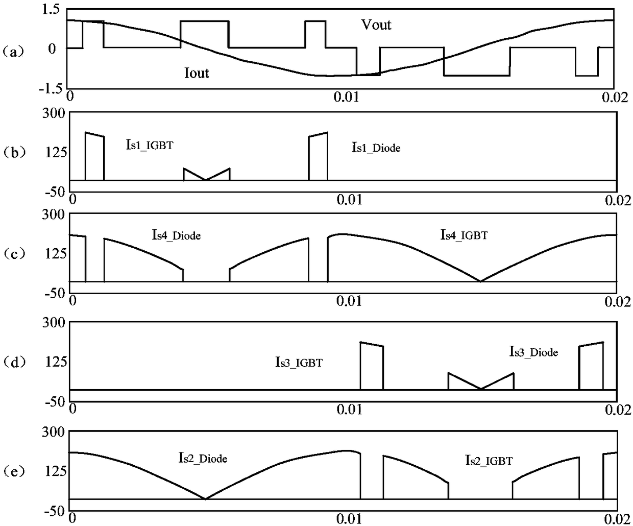
[0074] Example 1: Figure 7 The conduction diagram of the power semiconductor switch in the H bridge circuit provided by the present invention Figure 1 . Such as Figure 7 As shown, it is assumed that the control circuit 11 calculates the start time and stop time of the zero level of the output voltage Vout in every T / 2 work cycle, and determines that each T / 2 work cycle includes 3 Zero-level segments, that is, an odd number of zero-level segments. In this embodiment, Vout is a waveform diagram of the output voltage of the H-bridge circuit, and |Vout| is a waveform diagram of the absolute value of the output voltage of the H-bridge circuit. COM is the waveform diagram of the polarity of the output voltage of the H-bridge circuit. When the polarity of the output voltage Vout of the H-bridge circuit is positive (the positive pole comes from the modulation wave of the H-bridge circuit in the control circuit, when the modulation wave>0, the When the polarity of the H-bridge o...

example 2

[0080] Example 2: Figure 8 The conduction diagram of the power semiconductor switch in the H bridge circuit provided by the present invention Figure II . Such as Figure 8 As shown, it is assumed that the control circuit 11 calculates the start time and stop time of the zero level of the output voltage Vout in every T / 2 work cycle, and determines that each T / 2 work cycle includes 4 Zero-level segments, that is, an even number of zero-level segments. In this embodiment, Vout is a waveform diagram of the output voltage of the H-bridge circuit, and |Vout| is a waveform diagram of the absolute value of the output voltage of the H-bridge circuit. COM is a waveform diagram of the polarity of the output voltage of the H-bridge circuit. When the polarity of the output voltage Vout of the H-bridge circuit is positive, COM=1. When the polarity of the H-bridge output voltage is negative, COM=0. QS1 is the control signal waveform diagram of the upper power semiconductor switch S1 o...


PUM


Abstract

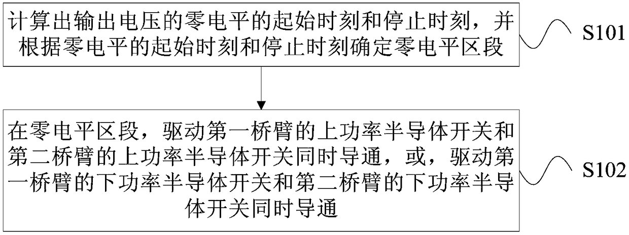
The invention provides a method for driving power semiconductor switches in an H-bridge circuit. The method comprises the steps of calculating a starting moment and a stopping moment of the zero levelof the output voltage, and determining a zero level section according to the starting moment and the stopping moment of the zero level; and in the zero level section, driving an upper power semiconductor switch of the first bridge arm and an upper power semiconductor switch of a second bridge arm to be simultaneously turned on, or driving a lower power semiconductor switch of the first bridge armand a lower power semiconductor switch of the second bridge arm to be simultaneously turned on. According to the method provided by the invention for driving the power semiconductor switches in the H-bridge circuit, the power semiconductor switches in the H-bridge circuit can be enabled to be similar in loss, and the service life of the H-bridge circuit is prolonged. Meanwhile, the consistency ofthe internal thermal design of a multi-level converter is facilitated, the cost and volume of a radiator adopted by the multi-level converter are reduced, and thus the cost and volume of the multi-level converter are reduced.

Description

technical field [0001] The invention relates to power supply technology, in particular to a driving method for a power semiconductor switch in an H bridge circuit. Background technique [0002] A multilevel converter is a converter that realizes high-voltage and high-power output by improving the topology of the converter itself, and is suitable for high-voltage and high-power applications. Wherein, the multilevel converter includes at least one H-bridge circuit, and each H-bridge circuit is composed of four power semiconductor switches. At present, multilevel converters usually use one of the following modulation methods to adjust the output voltage, such as: Sinusoidal Pulse Width Modulation (SPWM), Space Vector Pulse Width Modulation (SVPWM), specific Harmonic elimination modulation (SelectiveHarmonic Elimination PWM, SHEPWM), ladder wave / square wave modulation and other modulation methods. [0003] In the prior art, when the multilevel converter adopts the modulation m...

Claims


Application Information

Patent Timeline
IPC IPC(8): H02M1/088H02M7/483
CPCH02M1/088H02M7/483H02M1/0058Y02B70/10
Inventor 许炜沈定坤郑剑飞应建平胡志明田伟谢维蔚兰
Owner DELTA ELECTRONICS SHANGHAI CO LTD
Learn More