
Test optimization method of integrated circuit wafer

A technology of wafer testing and optimization method, which is applied in the direction of electronic circuit testing, automatic testing system, and electrical measurement. It can solve the problems of low wafer testing efficiency, improve testing efficiency, reduce testing time, and reduce the number of needles. Effect

Active Publication Date: 2018-09-11
SINO IC TECH
View PDF5 Cites 13 Cited by
  • Summary
  • Abstract
  • Description
  • Claims
  • Application Information

AI Technical Summary

Problems solved by technology

[0005] The present invention aims at the problem of low wafer test efficiency, and proposes an integrated circuit wafer test optimization method, which is applied in the integrated circuit wafer test process, by specifying the die coordinates to be tested in advance and storing them in the test system In the test process, the specified die is tested and adjusted in real time according to the test results, and finally the required test coordinate graphics are referenced to the generated test, thereby reducing test time, improving test efficiency, reducing the number of times used by test hardware, and improving the use of life

Method used


Image

  • Test optimization method of integrated circuit wafer
  • Test optimization method of integrated circuit wafer
  • Test optimization method of integrated circuit wafer

Examples


Embodiment Construction

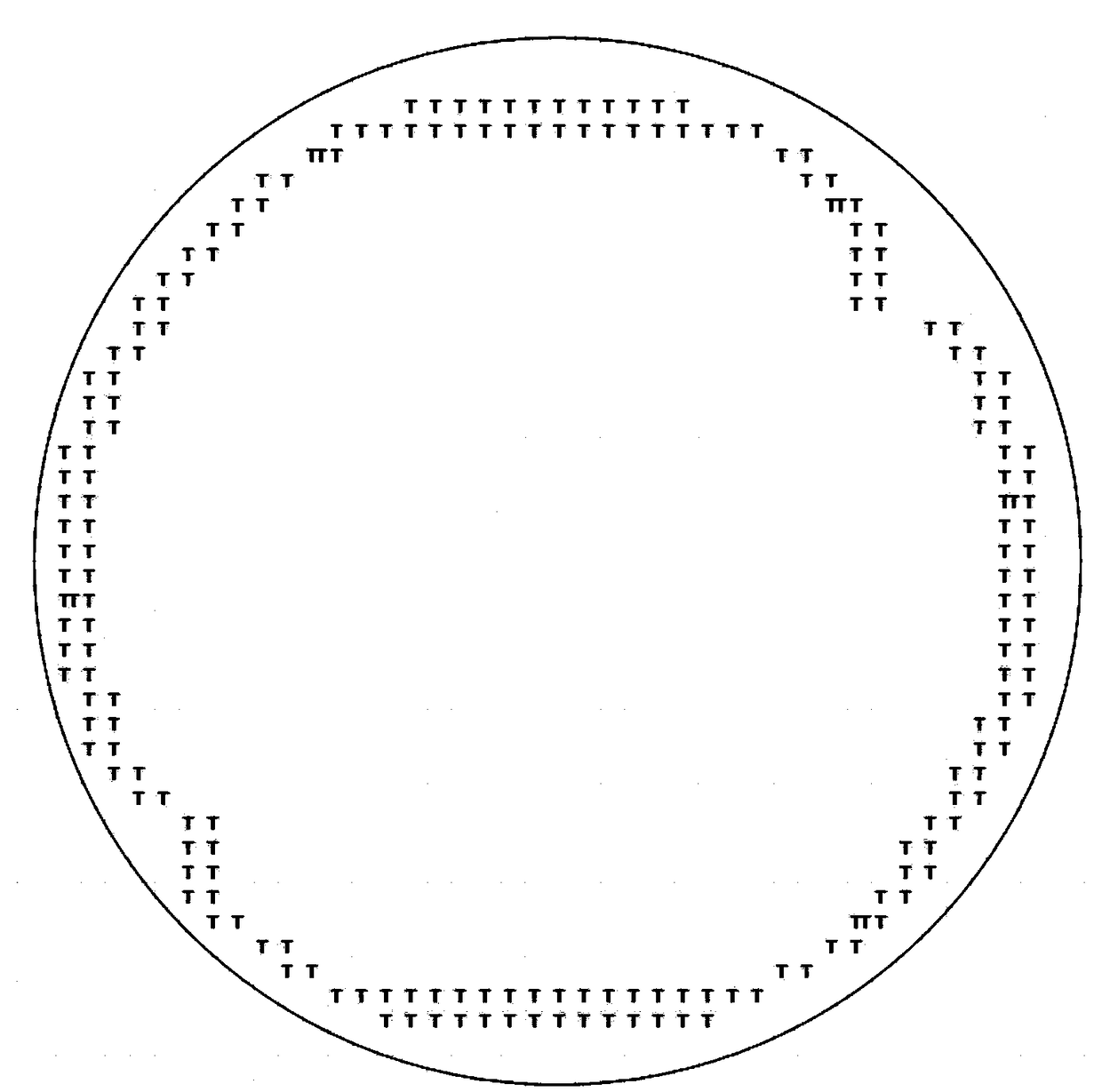
[0024] The yield rate of wafers caused by different types of chips and different manufacturing processes varies greatly. The yield rate of product A may be 99%, that of product B is 70%, and that of product C is only 20% to 30%. All dies of the entire wafer have been tested. For product A, it is necessary to pick out 1% of defective products, but it takes a lot of time to test the entire chip, and the test efficiency and cost ratio are poor.

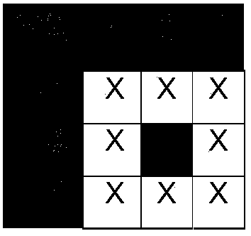
[0025] From the statistics of a large number of wafer test results, there is a large correlation between the failures of adjacent dies, that is, if the die at the coordinates of (X=100, Y=100) is in a failed state, with the die as the center, There is a high probability of failure in the surrounding 8 dies.

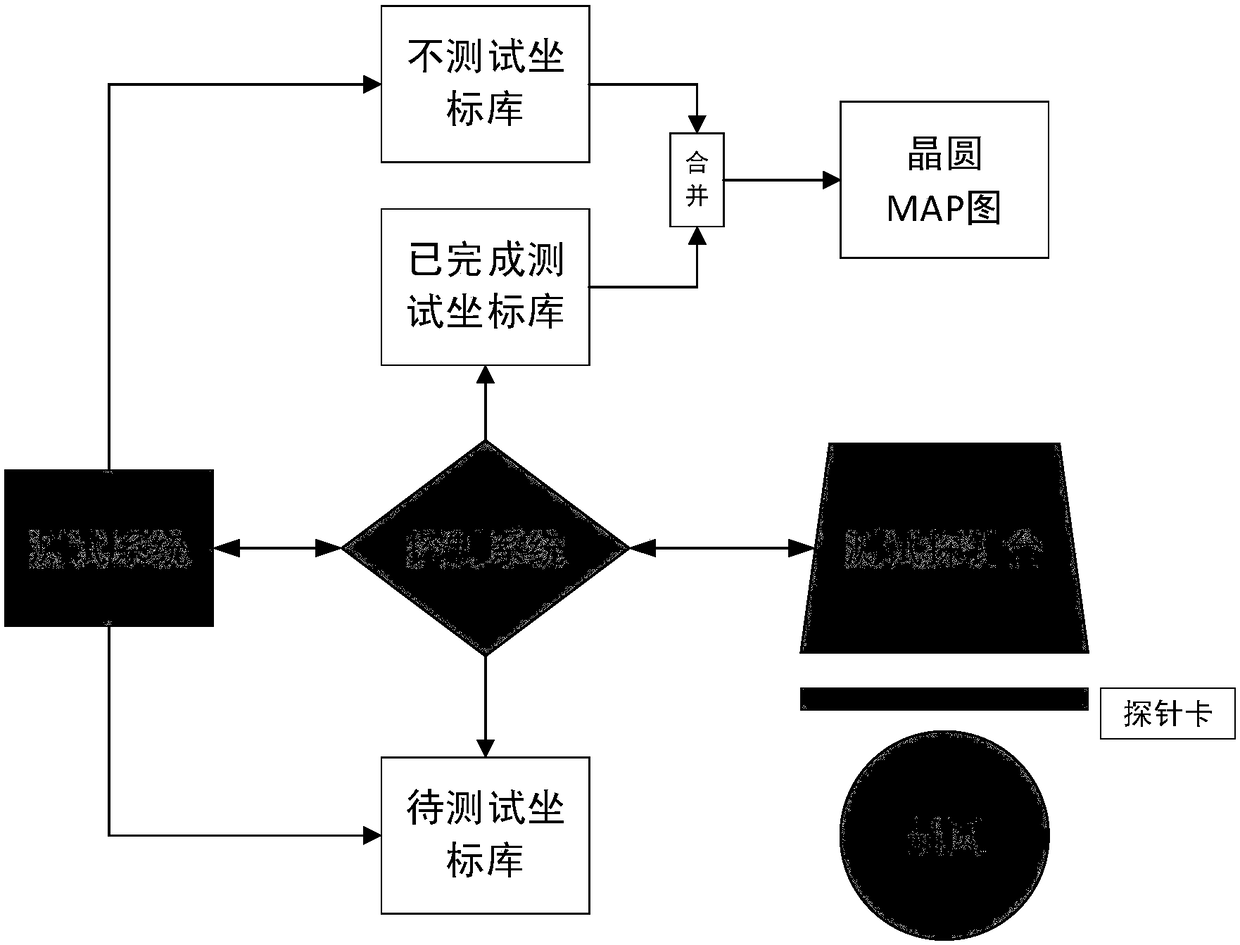
[0026] By pre-designating the coordinates of the dies to be tested in the wafer and storing them in the test system, the designated dies are tested during the test and adjusted in real time according to the test results, thereby re...


PUM


Abstract

The invention relates to a test optimization method of an integrated circuit wafer, and is applied to a test process of the integrated circuit wafer. The method includes: designating a die coordinatein need of a test on the wafer in advance and storing the coordinate in a test system, then testing the pre-designated die according to a design pattern in a test process and adjusting the range of the pre-designated coordinate in real time according to a current die test result, and finally obtaining a required test coordinate pattern to cover the most invalid die quantity with a most optimized scheme so that the test time is reduced, the test efficiency is improved, the usage frequency of test hardware is reduced, and the service lifetime is prolonged. According to the method, through propercoverage quantity calculation, a small quantity of FAIL chips flowing to package are obtained, and the packaging cost is not increased; besides, the test frequency of a probe card is reduced, and theservice lifetime of the hardware is prolonged.

Description

technical field [0001] The invention relates to a test and detection technology, in particular to an integrated circuit wafer test optimization method. Background technique [0002] ATE (Automatic Test Equipment): A semiconductor integrated circuit (IC) automatic tester, used to test the integrity of integrated circuit functions. Wafer: Wafer refers to the silicon wafer used in the production of silicon semiconductor integrated circuits. Because of its circular shape, it is called a wafer; it can be processed into various circuit element structures on the silicon wafer, and becomes a circuit with specific electrical properties. Functional IC products. Die: An independent integrated circuit chip on a wafer. [0003] Due to the advancement of integrated circuit design and manufacturing technology, the size of chips is getting smaller and smaller, but the size of silicon wafers has increased from 200mm to 300mm, and the number of chips that can be accommodated on a single waf...

Claims


Application Information

Patent Timeline
IPC IPC(8): G01R31/28
CPCG01R31/2851G01R31/2831G01R31/2834G01R31/2891
Inventor 王华张志勇凌俭波祁建华刘远华季海英
Owner SINO IC TECH
Features
  • Generate Ideas
  • Intellectual Property
  • Life Sciences
  • Materials
  • Tech Scout
  • Unparalleled Data Quality
  • Higher Quality Content
  • 60% Fewer Hallucinations
Learn More