Chuck device and semiconductor processing equipment

A chuck and base technology, applied in semiconductor/solid-state device manufacturing, electrical components, circuits, etc., can solve problems such as metal particle pollution, product quality impact, etc., to reduce metal pollution, improve temperature field and electric field uniformity, Improving the effect of uneven temperature distribution and steep electric field

Active Publication Date: 2018-09-14
BEIJING NAURA MICROELECTRONICS EQUIP CO LTD
View PDF7 Cites 1 Cited by
  • Summary
  • Abstract
  • Description
  • Claims
  • Application Information

AI Technical Summary

Problems solved by technology

[0006] However, since the conductive lower ring 140 is made of metal material, and there is a gap between the above-mentioned hot edge ring and the base 150, it is easy to cause metal particle pollution in the etching environment, thereby affecting the quality of the finished product

Method used


Image

  • Chuck device and semiconductor processing equipment
  • Chuck device and semiconductor processing equipment
  • Chuck device and semiconductor processing equipment

Examples


Embodiment Construction

[0029] In order for those skilled in the art to better understand the technical solution of the present invention, the chuck device and the semiconductor processing equipment provided by the present invention will be described in detail below with reference to the accompanying drawings.

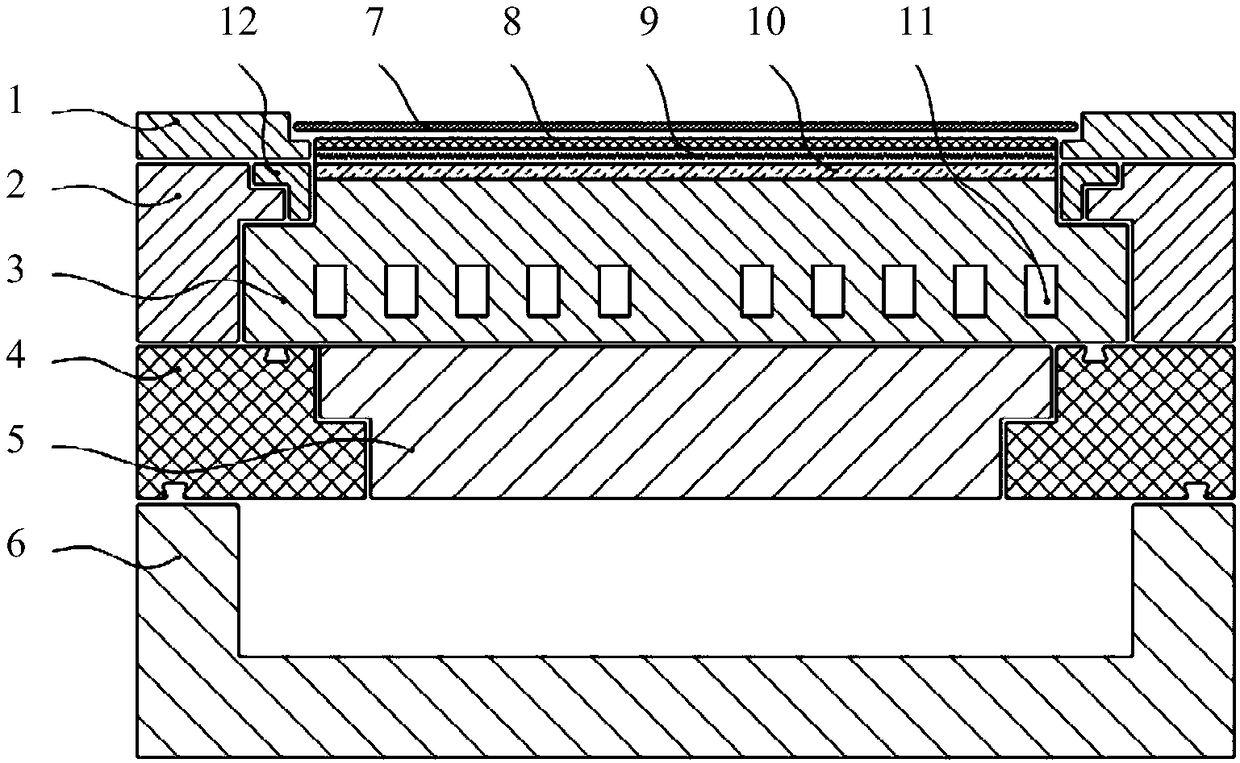
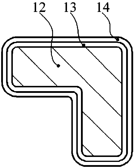
[0030] figure 2 It is a sectional view of the chuck device provided by the embodiment of the present invention. image 3 for figure 2 Cross-sectional view of a medium-heat edge ring. Please also refer to figure 2 and image 3 , The chuck device provided in this embodiment includes a base 3 , a base ring 2 , a focus ring 1 , an insulating ring 4 , an interface plate 5 , and a fixing member 6 . Wherein, an insulating layer 8, a heating layer 9 and a heat insulating layer 10 are sequentially arranged on the base 3 from top to bottom, wherein a DC electrode layer (not shown) is arranged in the insulating layer 8 to generate The electrostatic attraction fixes the chip 7 on the upper surfac...


PUM

PropertyMeasurementUnit
Thicknessaaaaaaaaaa
Thicknessaaaaaaaaaa

Abstract

The invention provides a chuck device and semiconductor processing equipment. The chuck device includes a base, a base ring, a focusing ring, and a thermal edge ring. The base includes a bearing surface used for bearing a wafer. The base ring is arranged around the sidewall of the base. The focusing ring is arranged on the base ring. The thermal edge ring is arranged between the base ring and thebase, and is close to the edge of the bearing surface. Furthermore, the thermal edge ring includes a metal body and an insulating layer covering the outer surface of the metal body. The chuck device provided by the invention can reduce metal pollution and particle pollution of the wafer on the premise of improving the uneven temperature distribution and steep electric field in a wafer edge region.

Description

technical field [0001] The invention relates to the field of semiconductor equipment manufacturing, in particular to a chuck device and semiconductor processing equipment. Background technique [0002] In the semiconductor manufacturing process, the plasma etching technology uses the physical effect produced by the bombardment of the wafer surface by high-energy ions, or uses the chemical interaction between the active free radicals in the plasma and the wafer surface, or the combination of the two , a technology to achieve the purpose of removing wafer material. A chuck device, such as an Electro Static Chuck (ESC), is provided in the plasma etching reaction chamber for fixing, supporting and transferring the wafer, and controlling the temperature of the wafer surface. [0003] The existing electrostatic chuck includes an insulating layer, a heating layer, a heat insulating layer and a base stacked in sequence from top to bottom, wherein a DC electrode layer is sintered in...

Claims


Application Information

Patent Timeline
IPC IPC(8): H01L21/67H01L21/683
CPCH01L21/67103H01L21/6833
Inventor 李一成彭宇霖曹永友
Owner BEIJING NAURA MICROELECTRONICS EQUIP CO LTD
Why Eureka
Try Eureka