Shifting register unit, driving method, Gate On Array and display device

A shift register and gate driving technology, applied in the fields of gate driving circuits and display devices, shift register units, and driving methods, can solve the problems of inconvenient adjustment of gate driving signal pulse width and the like

CN108564914AActive Publication Date: 2018-09-21BOE TECH GRP CO LTD +1
8 Cites 10 Cited by

Patent Information

Authority / Receiving Office
CN · China
Patent Type
Applications(China)
Current Assignee / Owner
Publication Date
2018-09-21

Smart Images

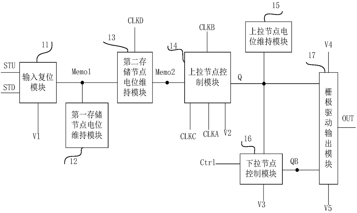
  • Figure 1
    Figure 1
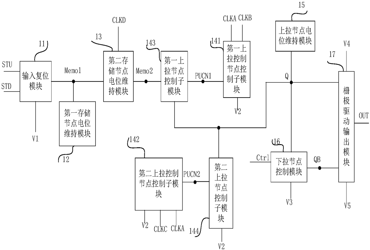
  • Figure 2
    Figure 2
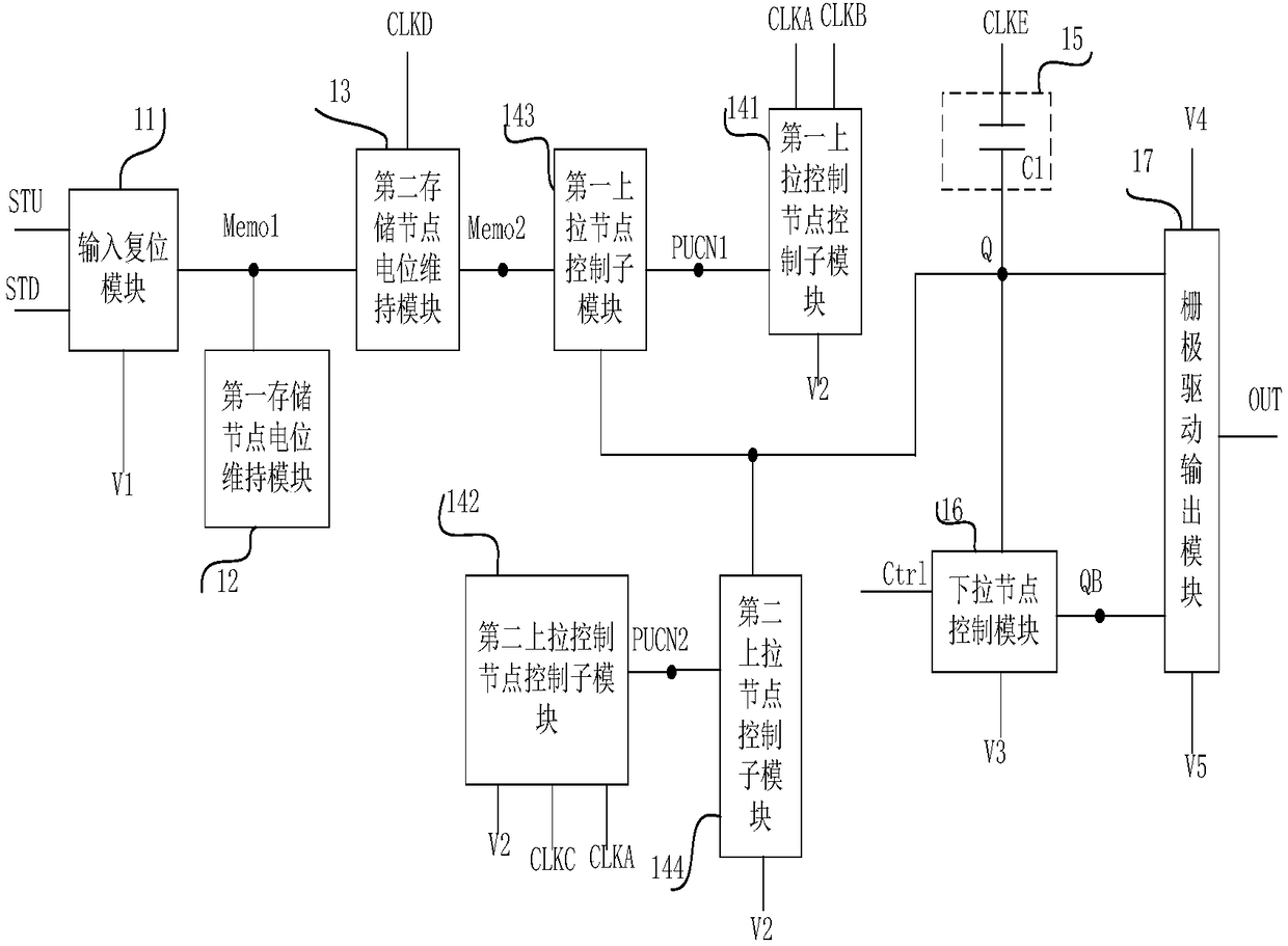
  • Figure 3
    Figure 3
Patent Text Reader

Abstract

The invention provides a shifting register unit, a driving method, a Gate On Array and a display device. The shifting register unit comprises an input resetting module, a first storing node potentialmaintaining module, a second storing node potential control module, a pull-up node control module, a pull-up node potential maintaining module, a pull-down node control module and a grid driving output module, wherein the pull-up node control module is used for controlling the potential of a pull-up node to be an active level under the control of a second storing node, a second clock signal inputend and a fourth clock signal input end, and controlling the pull-up node and a second voltage input end to be connected or disconnected under the control of a second clock signal input end and a third clock signal input end. Through the adoption of the shifting register unit disclosed by the invention, pulse modulation for a grid driving signal can be controlled by controlling a first clock signal and a second clock signal, so that the pulse width of the grid driving signal is adjustable.
Need to check novelty before this filing date? Find Prior Art

Description

technical field

[0001] The invention relates to the technical field of display driving, in particular to a shift register unit, a driving method, a gate driving circuit and a display device. Background technique

[0002] At present, the externally compensated gate drive circuit needs to match the pulse width of the gate output to be adjustable, and at the same time, it must solve the leakage problem of oxide TFT (oxide thin film transistor) and the weak output voltage load capacity caused by cascading. question. Moreover, the existing gate drive circuit cannot effectively store the pulse signal input by the shift register unit of the previous stage, thereby affecting the output of the gate drive signal of the present stage. Contents of the invention

[0003] The main purpose of the present invention is to provide a shift register unit, a driving method, a gate driving circuit and a display device, so as to solve the problem in the prior art that the pulse width of the out...

Examples

Embodiment Construction

[0086] The following will clearly and completely describe the technical solutions in the embodiments of the present invention with reference to the accompanying drawings in the embodiments of the present invention. Obviously, the described embodiments are only some, not all, embodiments of the present invention. Based on the embodiments of the present invention, all other embodiments obtained by persons of ordinary skill in the art without making creative efforts belong to the protection scope of the present invention.

[0087] The transistors used in all the embodiments of the present invention can be thin film transistors or field effect transistors or other devices with the same characteristics. In the embodiment of the present invention, in order to distinguish the two poles of the transistor except the gate, one pole is called the first pole, and the other pole is called the second pole. In actual operation, the first electrode may be a drain, and the second electrode may...