Silicon deep hole etching method

A silicon deep hole and stage technology, applied in the field of microelectronics, can solve the problems of deterioration of selectivity ratio, growth of grass in silicon pores, shrinkage of silicon pores, etc., and achieve the effect of improving the etching selectivity ratio

Active Publication Date: 2020-10-16
BEIJING NAURA MICROELECTRONICS EQUIP CO LTD
View PDF6 Cites 0 Cited by
  • Summary
  • Abstract
  • Description
  • Claims
  • Application Information

AI Technical Summary

Problems solved by technology

However, both of these methods will cause shrinkage or grass at the bottom of the silicon hole, because either increasing the chamber pressure in the deposition step or lowering the bottom electrode bias in the etching step will make the single-step deposition of the hole sidewall and Polymer weighting at the bottom of the pore, i.e. a thicker protective polymer layer is obtained during the deposition step
As the etching depth increases, the single-step etching rate slows down. When a certain etching depth is reached, the speed of single-step etching to remove the sidewall of the silicon hole and the polymer at the bottom of the silicon hole cannot keep up with the single-step deposition of polymer. The speed, that is, has entered the next cycle, which will cause the initial size of the etching to be small in the next cycle, so that after many cycles, the bottom of the silicon hole will shrink, and the higher chamber pressure will cause the silicon hole to shrink. The phenomenon of grass growing at the bottom of the hole, such as figure 1 shown
[0006] Although it is possible to increase the etching time or increase the bias voltage of the lower electrode, the subsequent deposition and etching cycle can be re-entered into the normal Bosch process cycle to ensure the recovery of the morphology, but this will cause the selectivity to deteriorate.

Method used


Image

  • Silicon deep hole etching method
  • Silicon deep hole etching method
  • Silicon deep hole etching method

Examples


Embodiment Construction

[0026] In order to enable those skilled in the art to better understand the technical solution of the present invention, the silicon deep hole etching method provided by the present invention will be described in detail below in conjunction with the accompanying drawings.

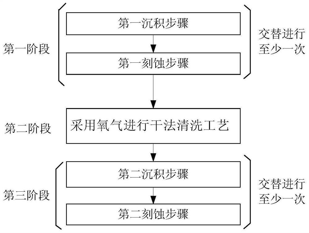
[0027] figure 2 A flow chart of a silicon deep hole etching method provided by an embodiment of the present invention. see figure 2 , silicon deep hole etching methods include:

[0028] In the first stage, the first deposition step and the first etching step are alternately performed at least once.

[0029] The specific process of the above-mentioned etching step or deposition step is as follows: simultaneously feed the process gas (etching gas or deposition gas) into the reaction chamber, and turn on the power supply of the upper electrode (such as a radio frequency power supply), and the power supply of the upper electrode is supplied to the reaction chamber Apply the power of the upper electrode to ...


PUM


Abstract

The invention provides a silicon deep hole etching method, and the method comprises a first stage: alternately performing a first deposition step and a first etching step for at least one time, wherein the lower electrode power at the first etching step is reduced through the increasing of the pressure of a cavity at the first deposition step and the first etching step, so as to improve the etching selection ratio; a second stage: performing the dry cleaning technique through oxygen, so as to remove the residual sediments and reaction products at the first stage; and a third stage: alternatelyperforming a second deposition step and a second etching step for at least one time, wherein the lower electrode power at the second etching step is reduced through the decreasing of the pressure ofthe cavity at the second deposition step and the second etching step, so as to obtain the required morphology and etching depth. The method provided by the invention can improve the etching selectionratio under the condition that the ideal etching morphology is obtained.

Description

technical field [0001] The invention relates to the technical field of microelectronics, in particular to a silicon deep hole etching method. Background technique [0002] In recent years, as MEMS devices and systems are more and more widely used in the fields of automobiles and consumer electronics, and the broad prospects of TSV (Through Silicon Etch, through hole etching) in the future packaging field, deep silicon etching technology has gradually become One of the hottest processes in the field of MEMS processing and TSV technology. Compared with the general deep silicon etching process [0003] The main difference between the deep silicon etching process and the general silicon etching process is that the etching depth of the deep silicon etching process is much larger than that of the general silicon etching process, and the etching depth of the deep silicon etching process is generally tens of microns It can even reach hundreds of microns, while the etching depth of...

Claims


Application Information

Patent Timeline
Patent Type & Authority Patents(China)
IPC IPC(8): H01L21/3065H01L21/02B81C1/00
CPCB81C1/00063B81C2201/0132H01L21/02057H01L21/30655
Inventor 胡竞之
Owner BEIJING NAURA MICROELECTRONICS EQUIP CO LTD
Why Eureka
Try Eureka