
Mechanical support device for semiconductor substrate processing microcavity

A substrate processing and mechanical support technology, applied in the field of chemical processing of semiconductor wafer surface, cleaning, etching and other similar processing devices, can solve the problems of increasing weight, increasing power, difficult level deviation, etc.

Active Publication Date: 2018-09-25
WUXI HUAYING MICROELECTRONICS TECH CO LTD
View PDF5 Cites 1 Cited by
  • Summary
  • Abstract
  • Description
  • Claims
  • Application Information

AI Technical Summary

Problems solved by technology

[0005] Although the above-mentioned improvements have improved the structural problems of the existing micro-processing chambers when wet processing wafers to a certain extent, the following problems still exist in the above-mentioned improvements: 1. the mobile unit is moved by using parts such as airbags, while the mobile unit moves At the same time, it is guided by the wheels set on the corners or edges of the lower support plate or the lower box, so it is difficult to ensure that there will be no horizontal deviation during the moving process, resulting in problems in the closure between the upper and lower chambers; and the precise processing of the corresponding holes in the box, but it is still necessary to accurately position the position of the wheels arranged on the corners or edges of the lower support plate or the lower box; At least one of the lower support plate or lower box needs to be dimensioned to the edge of the spacer struts, and the larger dimension adds extra weight and increases the power required for parts such as airbags to move the mobile unit

Method used


Image

  • Mechanical support device for semiconductor substrate processing microcavity
  • Mechanical support device for semiconductor substrate processing microcavity
  • Mechanical support device for semiconductor substrate processing microcavity

Examples


Embodiment Construction

[0023] "One embodiment" or "an embodiment" or "another embodiment" referred to in this specification means that specific features, structures or characteristics related to the embodiment can be included in at least one implementation of the present invention. The appearances of "in one embodiment" or "in another embodiment" in various places in this specification are not necessarily all referring to the same embodiment, nor are separate or selected embodiments mutually exclusive of other embodiments. "Multiple" in the present invention means two or more, and "several" means one or more. "And / or" in the present invention means "and" or "or".

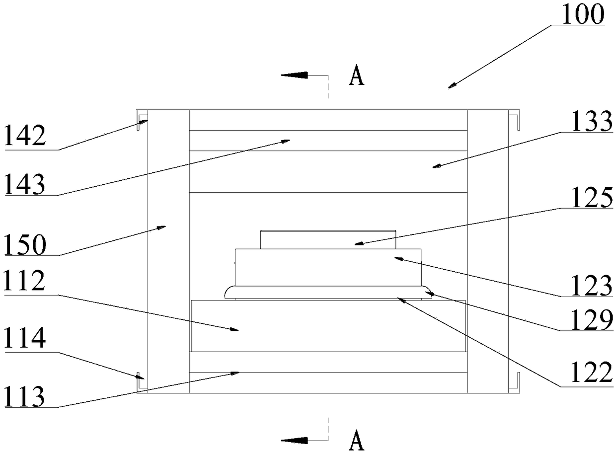
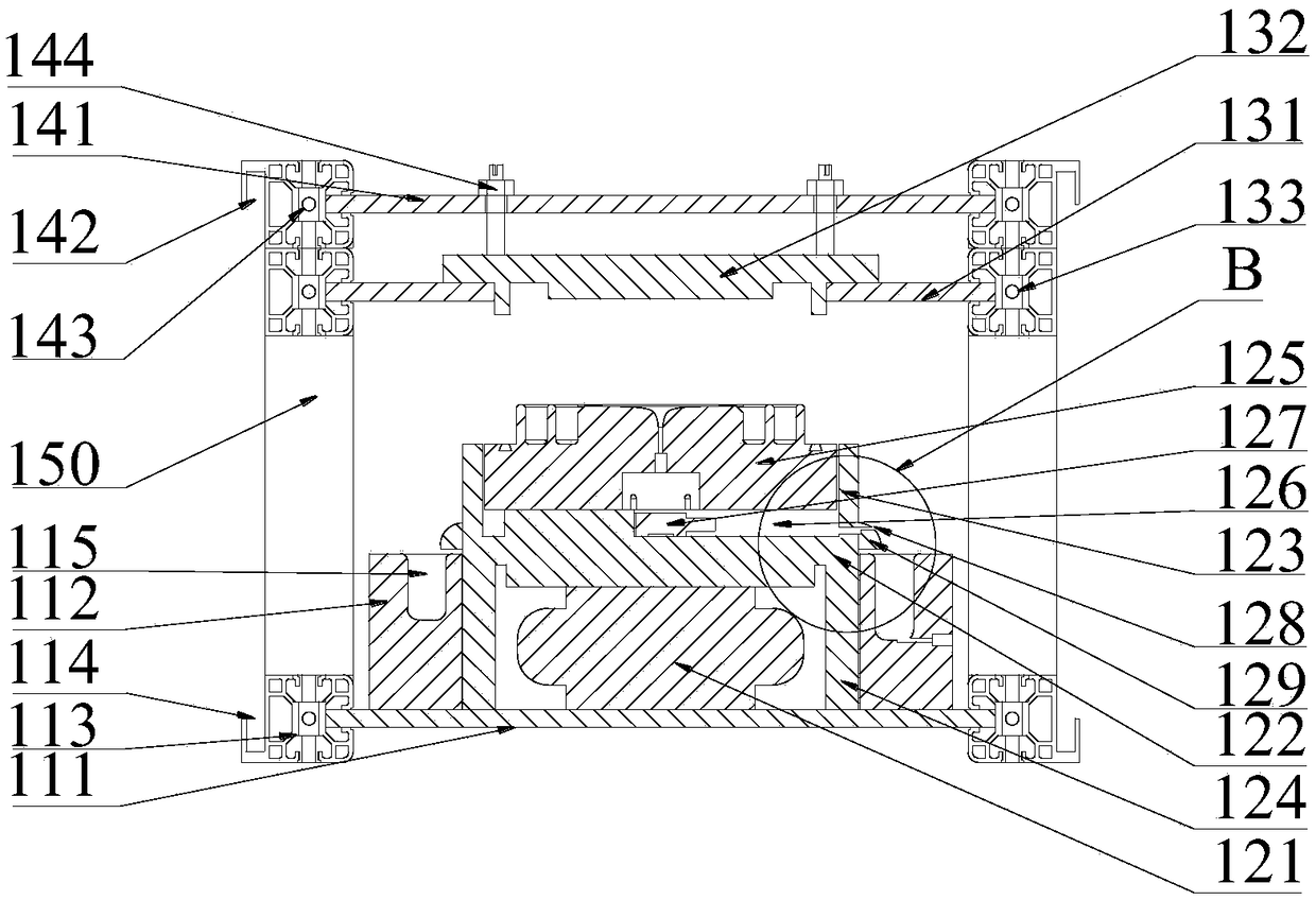
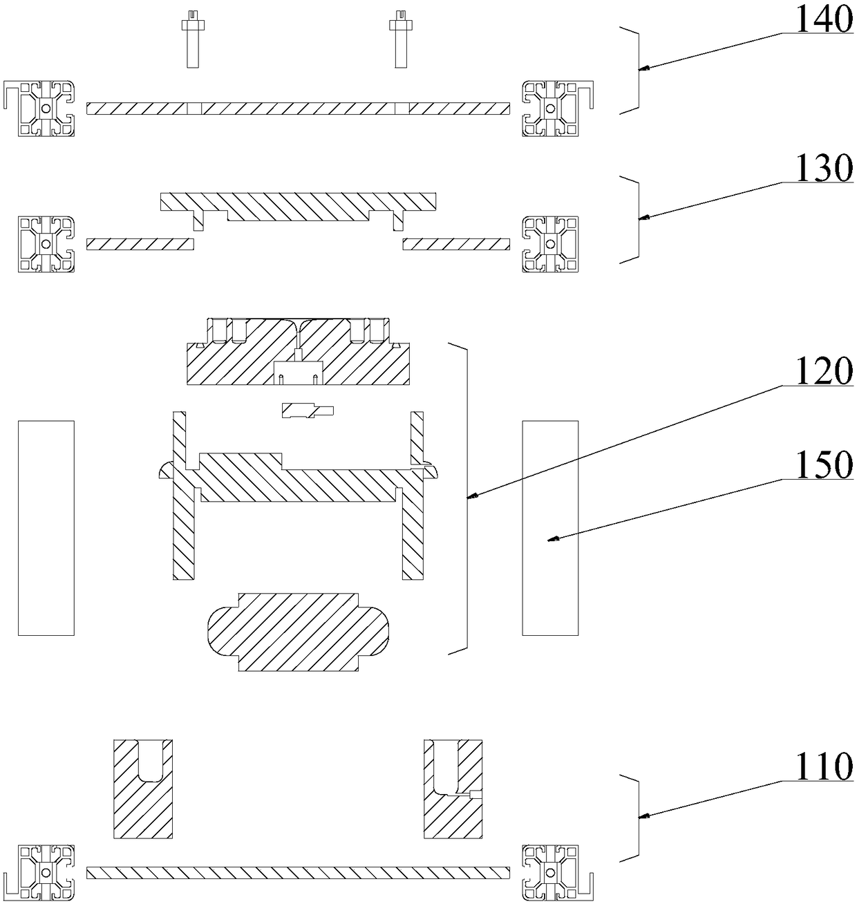
[0024] exist Figure 1 to Figure 5 The mechanical support device 100 of the semiconductor substrate processing microchamber of the present invention is schematically shown in .

[0025] Please refer to Figure 1-5 The mechanical support device 100 for the semiconductor substrate processing microchamber of the present invention may incl...


PUM


Abstract

The invention provides a mechanical support device for a semiconductor substrate processing microcavity, and the device comprises a horizontal first support plate, and a support ring which is fixedlydisposed above the first support plate; a moving seat which is in sliding sleeving fit with the support ring to form a sleeving fit space, wherein the interior of the sleeving fit space is provided with a drive unit which is fixedly connected with the support ring and the moving seat. The interior of an upper concave ring of the moving seat is provided with a lower cavity. The device also comprises an upper cavity which is used for forming the semiconductor substrate processing microcavity when the upper cavity makes contact with the lower cavity, wherein the upper cavity is fixed and adjustedto be level through a second support plate and a third support plate. According to the technical scheme of the invention, the drive unit controls the moving seat to move up and down relative to the support ring, so as to guide the lower cavity disposed in the moving seat and the upper cavity to close or open. Through a sleeving-fit structure between the support ring and the moving seat, the device directly controls the levelness of the moving seat during moving. Compared with the prior art, the device is simpler in structure, and is more stable in levelness.

Description

technical field [0001] The invention relates to the field of surface treatment of semiconductor wafers or similar workpieces, in particular a device for chemically treating the surface of semiconductor wafers, as well as cleaning, etching and other similar treatments. Background technique [0002] In the process of using wafers to produce integrated circuits, multiple cleaning, etching and other treatments are required. The above-mentioned treatment methods can be mainly divided into two types: dry method and wet method, among which wet method is the most widely used in the prior art. The existing wet process mainly includes chemical solution immersion and spray method. [0003] In the patent application filed by the applicant of this case with the publication number CN102737955A published on October 17, 2012, a method for wet processing of wafers using a micro-processing chamber is disclosed. In a microprocessing chamber, semiconductor wafers are closely received and proce...

Claims


Application Information

Patent Timeline
Patent Type & Authority Applications(China)
IPC IPC(8): H01L21/687
CPCH01L21/68764H01L21/68785
Inventor 温子瑛王吉王致凯
Owner WUXI HUAYING MICROELECTRONICS TECH CO LTD
Learn More